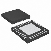
MAX1904ETJ+T Maxim Integrated Products, MAX1904ETJ+T Datasheet - Page 17

MAX1904ETJ+T
Manufacturer Part Number
MAX1904ETJ+T
Description
IC CNTRLR PWR SPLY LN 32-TQFN
Manufacturer
Maxim Integrated Products
Datasheet
1.MAX1904ETJ.pdf
(33 pages)
Specifications of MAX1904ETJ+T
Applications
Controller, Notebook Computers
Voltage - Input
4.2 ~ 30 V
Number Of Outputs
4
Voltage - Output
2.5 ~ 5 V
Operating Temperature
0°C ~ 85°C
Mounting Type
Surface Mount
Package / Case
32-TQFN Exposed Pad
Output Voltage
3.3 V, 5 V, 2.5 V to 5.5 V
Output Current
5 A
Input Voltage
4.2 V to 30 V
Mounting Style
SMD/SMT
Maximum Operating Temperature
+ 85 C
Minimum Operating Temperature
- 40 C
Lead Free Status / RoHS Status
Lead free / RoHS Compliant
The 2.5V reference (REF) is accurate to ±2% over tem-
perature, making REF useful as a precision system ref-
erence. Bypass REF to GND with 1µF minimum. REF
can supply up to 5mA for external loads. (Bypass REF
with a minimum 1µF/mA reference load current.)
However, if extremely accurate specifications for both
the main output voltages and REF are essential, avoid
loading REF more than 100µA. Loading REF reduces
the main output voltage slightly, because of the refer-
ence load-regulation error.
When the 5V main output voltage is above 4.5V, an
internal P-channel MOSFET switch connects CSL5 to
VL, while simultaneously shutting down the VL linear
regulator. This action bootstraps the IC, powering the
internal circuitry from the output voltage, rather than
through a linear regulator from the battery.
Bootstrapping reduces power dissipation due to gate
charge and quiescent losses by providing that power
from a 90%-efficient switch-mode source, rather than
from a much less efficient linear regulator.
Gate-drive voltage for the high-side N-channel switches
is generated by a flying-capacitor boost circuit (Figure 2).
The capacitor between BST_ and LX_ is alternately
charged from the VL supply and placed parallel to the
high-side MOSFET’s gate-source terminals. On startup,
the synchronous rectifier (low-side MOSFET) forces LX_
to 0V and charges the boost capacitors to 5V. On the
second half-cycle, the SMPS turns on the high-side MOS-
FET by closing an internal switch between BST_ and
DH_. This provides the necessary enhancement voltage
to turn on the high-side switch, an action that “boosts” the
5V gate-drive signal above the battery voltage.
Ringing at the high-side MOSFET gate (DH3 and DH5)
in discontinuous-conduction mode (light loads) is a nat-
ural operating condition. It is caused by residual ener-
gy in the tank circuit, formed by the inductor and stray
capacitance at the switching node, LX. The gate-drive
negative rail is referred to LX, so any ringing there is
directly coupled to the gate-drive output.
The current-limit circuit resets the main PWM latch and
turns off the high-side MOSFET switch whenever the
voltage difference between CSH and CSL exceeds
100mV. This limiting is effective for both current flow
directions, putting the threshold limit at ±100mV. The
tolerance on the positive current limit is ±20%, so the
external low-value sense resistor (R1) must be sized for
80mV/ I
500kHz Multi-Output, Low-Noise Power-Supply
PEAK
Current-Limiting and Current-Sense
Boost High-Side Gate-Drive Supply
, where I
______________________________________________________________________________________
PEAK
is the required peak-inductor
Inputs (CSH and CSL)
Controllers for Notebook Computers
(BST3 and BST5)
current to support the full load current, while compo-
nents must be designed to withstand continuous-
current stresses of 120mV/R1.
For breadboarding or for very-high-current applica-
tions, it may be useful to wire the current-sense inputs
with a twisted pair, rather than PC traces. (This twisted
pair need not be special; two pieces of wire-wrap wire
twisted together is sufficient.) This reduces the possible
noise picked up at CSH_ and CSL_, which can cause
unstable switching and reduced output current. The
CSL5 input also serves as the IC’s bootstrap supply
input. Whenever V
nects CSL5 to V
The SYNC input controls the oscillator frequency. Low
selects 333kHz; high selects 500kHz. SYNC can also
be used to synchronize with an external 5V CMOS or
TTL clock generator. SYNC has a guaranteed 400kHz
to 583kHz capture range. A high-to-low transition on
SYNC initiates a new cycle.
500kHz operation optimizes the application circuit for
component size and cost. 333kHz operation provides
increased efficiency, lower dropout, and improved
load-transient response at low input-output voltage dif-
ferences (see the Low-Voltage Operation section).
Holding SHDN low puts the IC into its 4µA shutdown
mode. SHDN is logic input with a threshold of about 1V
(the V
ic startup, bypass SHDN to GND with a 0.01µF capacitor
and connect it to V+ through a 220kΩ resistor.
Startup is controlled by RUN/ON3 and TIME/ON5 in
conjunction with SEQ. With SEQ tied to REF, the two
control inputs act as separate ON/OFF controls for
each supply. With SEQ tied to VL or GND, RUN/ON3
becomes the master ON/OFF control input and
TIME/ON5 becomes a timing pin, with the delay
between the two supplies determined by an external
capacitor. The delay is approximately 800µs/nF. The
3.3V supply powers up first if SEQ is tied to VL, and the
5V supply is first if SEQ is tied to GND. When driving
TIME/ON5 as a control input with external logic, always
place a resistor (>1kΩ) in series with the input. This
prevents possible crowbar current due to the internal
discharge pulldown transistor, which turns on in stand-
by mode and momentarily at the first power-up or in
shutdown mode.
TH
of an internal N-channel MOSFET). For automat-
L
.
CSL5
Power-Up Sequencing and
Oscillator Frequency and
> 4.5V, an internal switch con-
Synchronization (SYNC)
ON/ OFF Controls
Shutdown Mode
17


