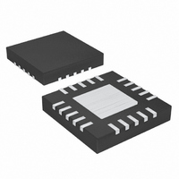
MAX1515ETG+T Maxim Integrated Products, MAX1515ETG+T Datasheet - Page 20

MAX1515ETG+T
Manufacturer Part Number
MAX1515ETG+T
Description
IC REG DDR LV 24-TQFN
Manufacturer
Maxim Integrated Products
Datasheet
1.MAX1515ETG.pdf
(24 pages)
Specifications of MAX1515ETG+T
Applications
Converter, DDR
Voltage - Input
1.3 ~ 3.6 V
Number Of Outputs
2
Voltage - Output
0.5 ~ 2.7 V
Operating Temperature
-40°C ~ 85°C
Mounting Type
Surface Mount
Package / Case
24-TQFN Exposed Pad
Lead Free Status / RoHS Status
Lead free / RoHS Compliant
Low-Voltage, Internal Switch,
Step-Down/DDR Regulator
The actual capacitance value required relates to the
physical size needed to achieve low ESR, as well as to
the chemistry of the capacitor technology. Thus, the
capacitor is usually selected by ESR and voltage rating
rather than by capacitance value (this is true of tanta-
lums, OS-CONs, polymers, and other electrolytics).
The inductor ripple current also impacts transient-
response performance, especially at low V
ferentials. Low inductor values allow the inductor
current to slew faster, replenishing charge removed
from the output filter capacitors by a sudden load step.
The worst-case output sag can be calculated from:
where ΔI
Typically, the maximum load transient is equal to the
maximum load current (ΔI
termination applications, the output must source and
sink current. In these applications, the actual peak-to-
peak transient current (ΔI
both the maximum source and sink load currents:
The amount of overshoot during a full-load to no-load
transient due to stored inductor energy can be calculat-
ed as:
When using the pulse-skipping source/sink feature
(MODE = V
voltage should not exceed or drop below the sink and
source (respectively) detection thresholds (V
±20mV).
The MAX1515 improves dropout performance by hav-
ing a maximum on-time of 10µs. When working with low
input voltages, the duty-factor limit must be calculated
using worst-case values for on- and off-times. Keep in
mind that transient-response performance of step-down
regulators operated too close to dropout is poor, and
20
V
SAG
______________________________________________________________________________________
ΔI
OUT
OUT
≈
2
+
CC
(
L
Δ
is the maximum load transient.
=
I
Δ
OUT
×
Applications Information
I
and SKIP = GND), the output transient
V
OUT OFF
I
C
C
SOURCE MAX
SOAR
OUT
OUT IN
L
t
+
(
V
V
≈
OUT OFF
(
OUT
OUT
2
C
−
(
t
Δ
OUT
V
) is defined as the sum of
)
I
Transient Response
OUT
OUT
= I
Dropout Operation
+
)
2
LOAD(MAX)
)
V
)
I
2
SINK MAX
OUT
+
L
V
2
(
OUT OFF
L
IN
×
). For DDR-
)
- V
C
t
OUT
OUT
2
REFIN
dif-
bulk output capacitance must often be added (see the
V
The absolute point of dropout is when the inductor cur-
rent ramps down during the off-time (ΔI
as it ramps up during the on-time (ΔI
ΔI
the inductor current higher in response to increased
load, and must always be greater than 1. As h
approaches 1, the absolute minimum dropout point, the
inductor current cannot increase as much during each
switching cycle and V
additional output capacitance is used.
A reasonable minimum value for h is 1.5, but adjusting
this up or down allows trade-offs between V
capacitance, and minimum operating voltage. For a
given value of h, the minimum operating voltage can be
calculated as:
where V
drops in the charge and discharge paths (see the
Frequency Variation with Output Current section),
t
is the programmed off-time. The absolute minimum
input voltage is calculated with h = 1.
If the calculated V
minimum input voltage, then t
output capacitance added to obtain an acceptable
V
late V
Dropout Design Example:
V
t
V
h = 1.5
By changing the voltage at REFIN, the MAX1515 can
be used in applications that require dynamic output-
voltage changes between two set points. An n-channel
MOSFET can be used to dynamically adjust the second
controller’s output voltage by changing the resistive
ON(MAX)
OFF
SAG
V
SAG
OUT
CHG
UP
IN MIN
(
V
/ΔI
= 1µs
IN MIN
. If operation near dropout is anticipated, calcu-
SAG
equation in the Design Procedure section).
= 2.5V
= V
(
DOWN
)
Dynamic Output-Voltage Transitions
CHG
=
is from the Electrical Characteristics, and t
DISCHG
to be sure of adequate transient response.
V
)
OUT
=
= 2.99V
and V
2 5
indicates the controller’s ability to slew
.
+
V
= 100mV
V
IN(MIN)
+
CHG
DISCHG
0 1
.
V
SAG
+
+
h t
is greater than the required
1 5 1
×
.
greatly increases unless
are the parasitic voltage
OFF
OFF
×
μ
×
must be reduced or
s
t
ON MAX
(
V
×
10
UP
OUT
( .
(
DOWN
2 5
μ
). The ratio h =
s
V
+
)
SAG
V
+
DISCHG
) as much
0 1
. )
, output
V
OFF
)


