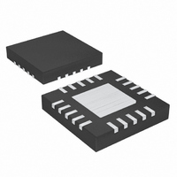
MAX1515ETG+T Maxim Integrated Products, MAX1515ETG+T Datasheet - Page 18

MAX1515ETG+T
Manufacturer Part Number
MAX1515ETG+T
Description
IC REG DDR LV 24-TQFN
Manufacturer
Maxim Integrated Products
Datasheet
1.MAX1515ETG.pdf
(24 pages)
Specifications of MAX1515ETG+T
Applications
Converter, DDR
Voltage - Input
1.3 ~ 3.6 V
Number Of Outputs
2
Voltage - Output
0.5 ~ 2.7 V
Operating Temperature
-40°C ~ 85°C
Mounting Type
Surface Mount
Package / Case
24-TQFN Exposed Pad
Lead Free Status / RoHS Status
Lead free / RoHS Compliant
Low-Voltage, Internal Switch,
Step-Down/DDR Regulator
Figure 6. Maximum Operating Frequency vs. Input Voltage
where:
C = 5nF
f
The combined conduction losses (PCL) in the two
power switches are approximated by:
where:
I
R
For typical DDR applications, use the recommended
component values in Table 1. For other applications,
use the recommended component values in Table 5, or
take the following steps:
1) Select the desired PWM-mode switching frequency.
2) Select the constant off-time as a function of input
3) Select R
4) Select the inductor as a function of output voltage,
The MAX1515 features a programmable PWM mode
switching frequency, which is set by the input and out-
put voltage and the value of R
high-side NMOS power switch off-time in PWM mode.
18
SW
OUT
NMOS
See Figure 6 for maximum operating frequency.
voltage, output voltage, and switching frequency.
off-time, and peak-to-peak inductor current.
= switching frequency
______________________________________________________________________________________
= load current
= NMOS switch on-resistance
1000
Programming the No-Load Switching
800
600
400
200
0
1.5
TOFF
MAXIMUM RECOMMENDED OPERATING
FREQUENCY vs. INPUT VOLTAGE
PCL = I
as a function of off-time.
V
2.0
OUT
= 1.25V
V
OUT
OUT
Frequency and Off-Time
V
= 1.5V
IN
2.5
Design Procedure
(V)
2
x R
NMOS
TOFF
V
OUT
V
3.0
OUT
V
OUT
= 1.8V
NO LOAD
= 2.5V
. R
= 0.9V
TOFF
3.5
sets the
Table 5. Recommended Component
Values (I
Use the following equation to select the off-time
according to the desired no-load switching frequency
in PWM mode:
where:
t
V
V
f
Select R
V
for R
0.35µs to 4.5µs.
The operating frequency of the MAX1515 in PWM mode
is determined primarily by t
V
where:
V
due to high-side FET R
V
path due to low-side FET R
OFF
PWM
IN
OUT
RTOFF
OUT
CHG
DISCHG
V
(V)
3.3
3.3
3.3
3.3
2.5
2.5
2.5
Frequency Variation with Output Current
IN
= the input voltage
= the programmed off-time
TOFF
= no-load switching frequency, PWM mode
= the output voltage
as shown in the following formula:
f
= the voltage drop in the inductor charge path
PWM
TOFF
is typically 1.1V and the recommended values
= the voltage drop in the inductor discharge
range from 33.2kΩ to 499kΩ for off-times of
V
OUT
(V)
2.5
1.8
1.5
1.2
1.8
1.5
1.2
OUT
R
=
according to the formula:
TOFF
= 3A)
t
OFF IN
t
OFF
=
f
(kHz)
PWM
(
400
400
480
420
430
320
440
V
(
V
t
IN
NMOS
OFF
=
−
−
NMOS
OFF
f
V
−
PWM
V
IN
V
and inductor DCR
0 035
OUT
CHG
(µH)
.
1.5
2.2
2.2
2.2
1.2
1.8
1.5
L
−
(set by R
and inductor DCR
V
×
OUT
−
μ
V
+
s
IN
)
V
1 00
CHG
110
V
C
(µF)
.
DISCHG
100
150
180
220
100
150
180
OUT
TOFF
k
μ
Ω
s
), V
)
R
IN
(kΩ)
49.9
49.9
110
110
150
110
110
TOFF
, and


