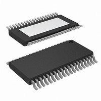
EL5525IREZ-T13 Intersil, EL5525IREZ-T13 Datasheet - Page 8

EL5525IREZ-T13
Manufacturer Part Number
EL5525IREZ-T13
Description
IC VREF GEN 18CH TFTLCD 38HTSSOP
Manufacturer
Intersil
Datasheet
1.EL5525IREZ.pdf
(10 pages)
Specifications of EL5525IREZ-T13
Applications
Converter, TFT, LCD
Voltage - Input
4.5 ~ 16.5 V
Number Of Outputs
18
Voltage - Output
0.5 ~ 14.95 V
Operating Temperature
-40°C ~ 85°C
Mounting Type
Surface Mount
Package / Case
38-TSSOP Exposed Pad, 38-eTSSOP, 38-HTSSOP
Lead Free Status / RoHS Status
Lead free / RoHS Compliant
takes to update the output depends on the timing at the V
and the state of the switches. It can take 1 to 18 clock cycles
to update each output.
For the sample and hold capacitor CH to maintain the
correct output voltage, the driving load shouldn’t be changed
at the rising edge of the OSC signal. Since at the rising edge
of the OSC clock, the refreshed switches are being opened,
if the load changes at that time, it will generate an error
output voltage. For a fixed load condition, the internal
oscillator can be used.
For the transient load condition, the external OSC mode
should be used to avoid the conflict between the rising edge
of the OSC signal and the changing load. So a timing delay
circuit will be needed to delay the OSC signal and avoid the
rising edge of the OSC signal and changing the load at the
same time.
Channel 3 --- sinking and sourcing 5mA current
Channel 2 --- EXT_OSC signal
Channel 1 --- V
In Figure Table 8 on page 8, the OSC signal is synchronized
to the load signal. The rising edge of the OSC signal is then
delayed by some amount of time and gives enough time for
CH to be charged to a new voltage before the switches are
opened.
FIGURE 9. CHANNEL TO CHANNEL REFRESH
FIGURE 8. TRANSIENT LOAD RESPONSE
OUT
8
IN
EL5525
Ch1 --- Output1
Ch3 --- Output2
Ch2 --- EXT_OSC
At the falling edge of the OSC, output 1 is being refreshed,
and one clock cycle later, output 2 is being refreshed. The
spike you see here is the response of the output amplifier
when the refreshed switches are closed. When driving a big
capacitor load, there will be ringing at the spikes because
the phase margin of the amplifier is decreased.
The speed of the external OSC signal shouldn’t be greater
than 70kHz because for the worst condition, it will take at
least 4µs to charge the sample and hold capacitor CH. The
pulse width has to be at least 4µs long. From our lab test, the
duty cycle of the OSC signal must be greater than 30%.
POWER DISSIPATION
With the 30mA maximum continues output drive capability
for each channel, it is possible to exceed the +125°C
absolute maximum junction temperature. Therefore, it is
important to calculate the maximum junction temperature for
the application to determine if load conditions need to be
modified for the part to remain in the safe operation.
The maximum power dissipation allowed in a package is
determined according to: Equation 2:
where:
• T
• T
• θ
• P
The maximum power dissipation actually produced by the IC
is the total quiescent supply current times the total power
supply voltage and plus the power in the IC due to the loads.
P
when sourcing, and:
when sinking.
Where:
• i = 18
• V
• I
• V
• I
P
P
DMAX
DMAX
DMAX
S
LOAD
JA
AMAX
JMAX
DMAX
S
OUT
= Quiescent current
= Supply voltage
= Thermal resistance of the package
=
=
i = Output voltage of the i channel
=
i = Load current of the i channel
= Maximum junction temperature
= Maximum ambient temperature
V
= Maximum power dissipation in the package
V
T
-------------------------------------------- -
S
JMAX
S
×
×
I
I
S
S
Θ
+
+
- T
JA
Σ V
Σ V
AMAX
[
(
(
OUT
S
- V
i
×
OUT
I
LOAD
i )
×
i
I
)
LOAD
i
]
September 21, 2010
FN7393.2
(EQ. 4)
(EQ. 2)
(EQ. 3)


