EL5525IREZ-T13 Intersil, EL5525IREZ-T13 Datasheet - Page 7
EL5525IREZ-T13
Manufacturer Part Number
EL5525IREZ-T13
Description
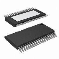
IC VREF GEN 18CH TFTLCD 38HTSSOP
Manufacturer
Intersil
Datasheet
1.EL5525IREZ.pdf
(10 pages)
Specifications of EL5525IREZ-T13
Applications
Converter, TFT, LCD
Voltage - Input
4.5 ~ 16.5 V
Number Of Outputs
18
Voltage - Output
0.5 ~ 14.95 V
Operating Temperature
-40°C ~ 85°C
Mounting Type
Surface Mount
Package / Case
38-TSSOP Exposed Pad, 38-eTSSOP, 38-HTSSOP
Lead Free Status / RoHS Status
Lead free / RoHS Compliant


Block Diagram
Channel Outputs
Each of the channel outputs has a rail-to-rail buffer. This
enables all channels to have the capability to drive to within
50mV of the power rails, (see Table Electrical Specifications
on page 2 for details).
When driving large capacitive loads, a series resistor should
be placed in series with the output. (Usually between 5Ω and
50Ω).
Each of the channels is updated on a continuous cycle, the
time for the new data to appear at a specific output will
depend on the exact timing relationship of the incoming data
to this cycle.
The best-case scenario is when the data has just been
captured and then passed on to the output stage
immediately; this can be as short as 48µs. In the worst-case
scenario, this will be 860µs for EL5525, when the data has
just missed the cycle at f_OSC = 21kHz.
When a large change in output voltage is required, the
change will occur in 2V steps, thus the requisite number of
timing cycles will be added to the overall update time. This
means that a large change of 16V can take between 6.8ms
and 7.2ms depending on the absolute timing relative to the
update cycle.
7
SCLK
ENA
SDI
REGISTERS
CHANNEL
18
EL5525
CONTROL IF
SOURCES
VOLTAGE
OSC_SELECT
Output Stage and the Use of External
Oscillator
The output voltage is generated from the DAC, which is V
in Figure 7. The refreshed switches are controlled by the
internal or external oscillator signal. When the OSC clock
signal is low, switches S
V
CH is being charged. When the OSC clock signal is high, the
refreshed switches S
voltage is maintained by CH. This refreshed process will
repeat every 18 clock cycles for each channel. The time
OUT
FIGURE 7. SIMPLIFIED OUTPUT SAMPLE AND HOLD AMP
1.3V
V
= V
IN
IN
and at the same time the sample and hold cap
STAGE FOR ONE CHANNEL
+
+
-
-
EXT_OSC
1
and S
REFH
OUTA
OUTB
OUTC
OUTD
OUTE
OUTP
OUTQ
OUTR
REFL
CAP
SDO
1
and S
S
1
2
S
are opened and the output
2
2
1.3V
are closed. The output
+
-
CH
OSC
September 21, 2010
V
OUT
FN7393.2
IN
Related parts for EL5525IREZ-T13
Image
Part Number
Description
Manufacturer
Datasheet
Request
R

Part Number:
Description:
IC VREF GEN 18CH TFTLCD 38HTSSOP
Manufacturer:
Intersil
Datasheet:
Part Number:
Description:
IC VREF GEN 18CH TFTLCD 38HTSSOP
Manufacturer:
Intersil
Datasheet:
Part Number:
Description:
IC VREF GEN 18CH TFTLCD 38HTSSOP
Manufacturer:
Intersil
Datasheet:

Part Number:
Description:
18-channel Tft-lcd Reference Voltage Generator
Manufacturer:
Intersil Corporation
Datasheet:
Part Number:
Description:
Intersil Corporation [CMOS Serial Controller Interface]
Manufacturer:
Intersil Corporation
Datasheet:
Part Number:
Description:
Manufacturer:
Intersil Corporation
Datasheet:
Part Number:
Description:
357-036-542-201 CARDEDGE 36POS DL .156 BLK LOPRO
Manufacturer:
Intersil Corporation
Datasheet:
Part Number:
Description:
1024-Word x 4-Bit LSI Static RAM
Manufacturer:
Intersil Corporation
Datasheet:
Part Number:
Description:
General Purpose NPN Transistor Arrays FN341.4
Manufacturer:
Intersil Corporation
Datasheet:
Part Number:
Description:
CMOS 16-Bit Microprocessor
Manufacturer:
Intersil Corporation
Datasheet:
Part Number:
Description:
Manufacturer:
Intersil Corporation
Datasheet:
Part Number:
Description:
Manufacturer:
Intersil Corporation
Datasheet:
Part Number:
Description:
Manufacturer:
Intersil Corporation
Datasheet:
Part Number:
Description:
Manufacturer:
Intersil Corporation
Datasheet:
Part Number:
Description:
CMOS 6-Bit Latch and Decoder Memory Interfaces
Manufacturer:
Intersil Corporation
Datasheet: