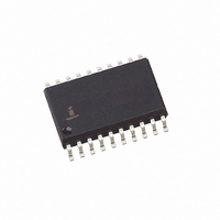
HIP6004BCBZ Intersil, HIP6004BCBZ Datasheet - Page 6

HIP6004BCBZ
Manufacturer Part Number
HIP6004BCBZ
Description
IC CTRLR PWM VOLTAGE MON 20-SOIC
Manufacturer
Intersil
Specifications of HIP6004BCBZ
Applications
Controller, Intel Pentium®, II, Pro
Voltage - Input
5V, 12V
Number Of Outputs
1
Voltage - Output
1.3 ~ 3.5 V
Operating Temperature
0°C ~ 70°C
Mounting Type
Surface Mount
Package / Case
20-SOIC (7.5mm Width)
Input Voltage
12V
Output Voltage
3.5V
Supply Voltage Range
10.8V To 13.2V
Digital Ic Case Style
SOIC
No. Of Pins
20
Operating Temperature Range
0°C To +70°C
Filter Terminals
SMD
Rohs Compliant
Yes
Control Mode
Voltage
Lead Free Status / RoHS Status
Lead free / RoHS Compliant
GND (Pin 11)
Signal ground for the IC. All voltage levels are measured
with respect to this pin.
PGOOD (Pin 12)
PGOOD is an open collector output used to indicate the
status of the converter output voltage. This pin is pulled low
when the converter output is not within ±10% of the
DACOUT reference voltage. Exception to this behavior is the
‘11111’ VID pin combination which disables the converter; in
this case PGOOD asserts a high level.
PHASE (Pin 13)
Connect the PHASE pin to the upper MOSFET source. This
pin is used to monitor the voltage drop across the MOSFET
for over-current protection. This pin also provides the return
path for the upper gate drive.
UGATE (Pin 14)
Connect UGATE to the upper MOSFET gate. This pin
provides the gate drive for the upper MOSFET.
BOOT (Pin 15)
This pin provides bias voltage to the upper MOSFET driver.
A bootstrap circuit may be used to create a BOOT voltage
suitable to drive a standard N-Channel MOSFET.
PGND (Pin 16)
This is the power ground connection. Tie the lower MOSFET
source to this pin.
LGATE (Pin 17)
Connect LGATE to the lower MOSFET gate. This pin
provides the gate drive for the lower MOSFET.
V
Provide a 12V bias supply for the chip to this pin.
OVP (Pin 19)
The OVP pin can be used to drive an external SCR in the
event of an overvoltage condition. Output rising 15% more
than the DAC-set voltage triggers a high output on this pin
and disables PWM gate drive circuitry.
RT (Pin 20)
This pin provides oscillator switching frequency adjustment.
By placing a resistor (R
200kHz switching frequency is increased according to the
following equation:
Conversely, connecting a pull-up resistor (R
to V
following equation:
Fs
Fs
CC
≈
≈
CC
200kHz
200kHz
(Pin 18)
reduces the switching frequency according to the
+
–
-------------------- -
R
-------------------- -
R
4 x 10
5 x 10
T
T
(
(
kΩ
kΩ
6
7
)
)
T
) from this pin to GND, the nominal
(R
(R
T
T
to 12V)
to GND)
6
T
) from this pin
HIP6004B
Functional Description
Initialization
The HIP6004B automatically initializes upon receipt of power.
Special sequencing of the input supplies is not necessary. The
Power-On Reset (POR) function continually monitors the input
supply voltages. The POR monitors the bias voltage at the V
pin and the input voltage (V
OCSET is equal to V
current protection). The POR function initiates soft start
operation after both input supply voltages exceed their POR
thresholds. For operation with a single +12V power source, V
and V
exceed the rising V
Soft Start
The POR function initiates the soft start sequence. An internal
10µA current source charges an external capacitor (C
the SS pin to 4V. Soft start clamps the error amplifier output
(COMP pin) and reference input (+ terminal of error amp) to the
SS pin voltage. Figure 3 shows the soft start interval with
C
pin) controls the converter’s output voltage. At t
the SS voltage reaches the valley of the oscillator’s triangle
wave. The oscillator’s triangular waveform is compared to the
ramping error amplifier voltage. This generates PHASE pulses
of increasing width that charge the output capacitor(s). This
interval of increasing pulse width continues to t
output voltage, the clamp on the reference input controls the
output voltage. This is the interval between t
At t
output voltage is in regulation. This method provides a rapid
and controlled output voltage rise. The PGOOD signal toggles
‘high’ when the output voltage (V
DACOUT. The 2% hysteresis built into the power good
comparators prevents PGOOD oscillation due to nominal
output voltage ripple.
SS
0V
0V
0V
3
= 0.1µF. Initially the clamp on the error amplifier (COMP
the SS voltage exceeds the DACOUT voltage and the
CC
are equivalent and the +12V power source must
FIGURE 3. SOFT START INTERVAL
SOFT-START
(1V/DIV)
CC
IN
threshold before POR initiates operation.
t
less a fixed voltage drop (see over-
1
PGOOD
(2V/DIV)
IN
TIME (5ms/DIV)
) on the OCSET pin. The level on
t
2
SEN
pin) is within ±5% of
t
3
2
and t
2
1
. With sufficient
in Figure 3,
VOLTAGE
OUTPUT
3
(1V/DIV)
in Figure 3.
SS
) on
CC
IN


