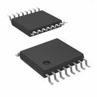
LM5026MTX/NOPB National Semiconductor, LM5026MTX/NOPB Datasheet - Page 16

LM5026MTX/NOPB
Manufacturer Part Number
LM5026MTX/NOPB
Description
CURRENT MODE-ACTIVE RESET
Manufacturer
National Semiconductor
Series
PowerWise®r
Datasheet
1.LM5026MTNOPB.pdf
(22 pages)
Specifications of LM5026MTX/NOPB
Pwm Type
Current Mode
Number Of Outputs
2
Frequency - Max
1MHz
Duty Cycle
92.5%
Voltage - Supply
13 V ~ 100 V
Buck
Yes
Boost
Yes
Flyback
Yes
Inverting
Yes
Doubler
No
Divider
No
Cuk
No
Isolated
Yes
Operating Temperature
-40°C ~ 125°C
Package / Case
16-TSSOP
Frequency-max
1MHz
For Use With
LM5026EVAL - BOARD EVALUATION LM5026
Lead Free Status / RoHS Status
Lead free / RoHS Compliant
Other names
*LM5026MTX/NOPB
LM5026MTX
Q2535472
LM5026MTX
Q2535472
Available stocks
Company
Part Number
Manufacturer
Quantity
Price
Company:
Part Number:
LM5026MTX/NOPB
Manufacturer:
TI
Quantity:
3 000
www.national.com
OSCILLATOR (RT, SYNC)
Oscillator (RT, SYNC) The oscillator frequency is generally
selected in conjunction with the design of the system mag-
netic components along with the volume and efficiency goals
for a given power converter design. The total RT resistance
at the RT pin sets the oscillator frequency. The RT resistors
should be one of the first components placed and connected
when designing the PC board. Direct, short connections to
each side of the RT resistors (RT, DCL and AGND pins) are
recommended .
The SYNC pin can be used to synchronize the internal oscil-
lator to an external clock. An open drain output is the recom-
mended interface from the external clock to the SYNC pin.
The clock pulse width should be greater than 15 ns. The ex-
ternal clock must be a higher frequency than the free running
frequency set by the RT resistor. Multiple LM5026 devices
can be synchronized together simply by connecting the de-
vices SYNC pins together. Care should be taken to ensure
the ground potential differences between devices are mini-
mized. In this configuration all of the devices will be synchro-
nized to the highest frequency device.
VOLTAGE FEEDBACK (COMP)
The COMP pin is designed to accept the voltage loop feed-
back error signal from the regulated output via an error am-
FIGURE 14. Remote Standby and Disable Control
FIGURE 13. Basic UVLO Configuration
16
plifier and (typically) an optocoupler. In a typical configuration,
VOUT is compared to a precision reference voltage by the
error amplifier. The amplifier’s output drives the optocoupler,
which in turn drives the COMP pin. The parasitic capacitance
of the optocoupler often limits the achievable loop bandwidth
for a given power converter. The optocoupler LED and de-
tector junction capacitance produce a low frequency pole in
the voltage regulation loop. The LM5026 current controlled
optocoupler interface (COMP) previously described, greatly
increases the pole frequency associated with the optocou-
pler.
CURRENT SENSE (CS)
The CS pin receives an input signal representative of the
transformer primary current, either from a current sense
transformer
source of the primary switch
sensed current creates a ramping voltage across R1, while
the R
C
and the ground connection from the current sense trans-
former, or R1, should be a dedicated track to the AGND pin.
The current sense components must provide >0.5V at the CS
pin when an over-current condition exists.
F
should be as physically close to the LM5026 as possible,
F
/C
F
filter suppresses noise and transients. R1, R
(Figure
15) or from a resistor in series with the
20147924
(Figure
20147925
16). In both cases the
F
and


