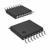
LM5026MTX/NOPB National Semiconductor, LM5026MTX/NOPB Datasheet - Page 11

LM5026MTX/NOPB
Manufacturer Part Number
LM5026MTX/NOPB
Description
CURRENT MODE-ACTIVE RESET
Manufacturer
National Semiconductor
Series
PowerWise®r
Datasheet
1.LM5026MTNOPB.pdf
(22 pages)
Specifications of LM5026MTX/NOPB
Pwm Type
Current Mode
Number Of Outputs
2
Frequency - Max
1MHz
Duty Cycle
92.5%
Voltage - Supply
13 V ~ 100 V
Buck
Yes
Boost
Yes
Flyback
Yes
Inverting
Yes
Doubler
No
Divider
No
Cuk
No
Isolated
Yes
Operating Temperature
-40°C ~ 125°C
Package / Case
16-TSSOP
Frequency-max
1MHz
For Use With
LM5026EVAL - BOARD EVALUATION LM5026
Lead Free Status / RoHS Status
Lead free / RoHS Compliant
Other names
*LM5026MTX/NOPB
LM5026MTX
Q2535472
LM5026MTX
Q2535472
Available stocks
Company
Part Number
Manufacturer
Quantity
Price
Company:
Part Number:
LM5026MTX/NOPB
Manufacturer:
TI
Quantity:
3 000
The rising edge overlap or deadtime and the falling edge
overlap or deadtime are identical and are independent of op-
erating frequency or duty cycle. The magnitude of the overlap/
deadtime can be calculated as follows:
Overlap Time = 2.8 x R
Deadtime = 2.9 x R
With R
Gate Driver Outputs
The LM5026 provides two gate driver outputs, the main power
switch control (OUT_A) and the active clamp switch control
(OUT_B). The main gate driver features a compound config-
uration, consisting of both MOS and bipolar devices, which
provide superior gate drive characteristics. The bipolar device
provides most of the drive current capability and sinks a rel-
atively constant current, which is ideal for driving large power
MOSFETs. As the switching event nears conclusion and the
bipolar device saturates, the internal MOS device provides a
low impedance to compete the switching event.
During turn-off at the Miller plateau region, typically between
2V - 4V, the voltage differential between the output and PGND
is small and the current source characteristic of the bipolar
device is beneficial to reduce the transition time. During turn-
on, the resistive characteristics of a purely MOS gate driver
is adequate since the supply to output voltage differential is
fairly large in the Miller region.
SET
in K Ohms and overlap / deadtime in nanoseconds
FIGURE 3. Compound Gate Driver
SET
+ 14
SET
+ 2
FIGURE 2. PWM Output Phasing / Timing
20147914
11
PWM Comparator/Slope
Compensation
The PWM comparator modulates the pulse width of the con-
troller output by comparing the current sense ramp signal to
the loop error signal. This comparator is optimized for speed
in order to achieve minimum controllable duty cycles. The
loop error signal is input into the controller in the form of a
control current into the COMP pin. The COMP pin control
current is internally mirrored by a matched pair of NPN tran-
sistors which sink current through a 5 kΩ resistor connected
to the 5V reference. The resulting error signal passes through
a 1.4V level shift and a gain reducing 3:1 resistor divider be-
fore being applied to the pulse width modulator.
The opto-coupler detector can be connected between the
REF pin and the COMP pin. Because the COMP pin is con-
trolled by a current input, the potential difference across the
optocoupler detector is nearly constant. The bandwidth limit-
ing phase delay which is normally introduced by the signifi-
cant capacitance of the opto-coupler is greatly reduced.
Greater system loop bandwidth can be realized, since the
bandwidth-limiting pole associated with the opto-coupler is
now at a much higher frequency. The PWM comparator po-
larity is configured such that with no current into the COMP
pin, the controller produces the maximum duty cycle at the
main gate driver output.
20147913
www.national.com


