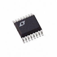
LT1950EGN Linear Technology, LT1950EGN Datasheet - Page 12

LT1950EGN
Manufacturer Part Number
LT1950EGN
Description
IC CTLR PWM SGL SWITCH 16-SSOP
Manufacturer
Linear Technology
Datasheet
1.LT1950IGNPBF.pdf
(20 pages)
Specifications of LT1950EGN
Pwm Type
Current Mode
Number Of Outputs
1
Frequency - Max
560kHz
Duty Cycle
97%
Voltage - Supply
3 V ~ 25 V
Buck
No
Boost
Yes
Flyback
Yes
Inverting
No
Doubler
No
Divider
No
Cuk
No
Isolated
Yes
Operating Temperature
-40°C ~ 125°C
Package / Case
16-SSOP
Frequency-max
560kHz
Lead Free Status / RoHS Status
Contains lead / RoHS non-compliant
Available stocks
Company
Part Number
Manufacturer
Quantity
Price
Company:
Part Number:
LT1950EGN
Manufacturer:
LT
Quantity:
10 000
Part Number:
LT1950EGN
Manufacturer:
LINEAR/凌特
Quantity:
20 000
Part Number:
LT1950EGN#PBF
Manufacturer:
LINEAR/凌特
Quantity:
20 000
Part Number:
LT1950EGN#TRPBF
Manufacturer:
LINEAR/凌特
Quantity:
20 000
LT1950
APPLICATIO S I FOR ATIO
(V)
(A)
(A)
(V)
12
N-channel power MOSFET even though V
low. High GATE drive voltage reduces MOSFET R
improves efficiency and increases the range of MOSFETs
that can be selected. A small switching regulator at the
BOOST pin, with fixed current limit and fixed off time,
generates the V
connected between the BOOST pin and V
the BOOST pin will draw current until approximately
125mA is reached, turn off for 0.5µs and then turn back on.
The cycle is repeated for as long as the switcher is enabled.
By using a diode connected from BOOST to V
capacitor from V
inductor is transferred to the V
time of the internal switcher. An auxiliary boost converter
is realized providing a supply to the V
inductor current, V
waveforms are shown in Figure 5. When V
the internal switcher is disabled. Since V
output driver of the LT1950, switching at the GATE pin will
eventually discharge the V
a lower level of approximately 10V. At this level the internal
switcher is re-enabled and switches until V
0.25
0.25
12
10
15
0
0
0
Figure 5. V
IN2
IN2
5µs/DIV
IN2
U
IN2
Generation Using the BOOST Pin
to ground, energy from the external
supply. With an external inductor
voltage and BOOST pin voltage
U
IN2
capacitor until V
BOOST
IN2
V
IN2
I
I
D1
L1
capacitor during the off-
W
MIN
3V
IN2
LT1950
IN
IN
IN2
IN2
pin. The typical
V
BOOST
BOOST
(see Figure 5),
IN
voltage is very
IN2
V
V
reaches 11V,
IN2
IN2
supplies the
IN2
returns to
U
IN2
reaches
DS(ON)
L1
and a
D1
C1
1950 F05
,
11V. This hysteretic (burst mode) operation for the inter-
nal switcher minimizes power dissipation from V
The V
LT1950 control circuitry. It is available for external use
with maximum current capability of 2.5mA. The pin should
be bypassed to ground using a 0.1µF capacitor. Internal
undervoltage lockout thresholds for V
proximately 2.6V and 6.8V respectively must be exceeded
before V
Programming Oscillator Frequency
The oscillator frequency of the LT1950 is programmed
using an external resistor connected between the R
and ground. Figure 6 shows typical f
values. The LT1950 is programmable for a free-running
oscillator frequency in the range of 100kHz to 500kHz.
Stray capacitance and potential noise pickup on the R
pin should be minimized by placing the R
close as possible to the R
the R
R
(analog ground) pin.
OSC
OSC
REF
resistor should be returned directly to the GND
REF
Figure 6. Oscillator Frequency (f
node as small as possible. The ground side of the
output is a 2.5V reference supplying most of the
becomes active.
500
450
400
350
300
250
200
150
100
50
100 150
200
OSC
R
250
OSC
pin and keeping the area of
(kΩ)
300 350
OSC
OSC
400 450 500
IN
) vs R
vs R
and V
OSC
1950 F06
OSC
OSC
resistor as
IN2
resistor
IN
OSC
of ap-
.
1950fa
OSC
pin


