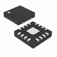
MAX8598ETE+ Maxim Integrated Products, MAX8598ETE+ Datasheet - Page 22

MAX8598ETE+
Manufacturer Part Number
MAX8598ETE+
Description
IC CNTRLR STP DWN LDO 16-TQFN
Manufacturer
Maxim Integrated Products
Datasheet
1.MAX8597ETP.pdf
(24 pages)
Specifications of MAX8598ETE+
Pwm Type
Controller
Number Of Outputs
1
Frequency - Max
1.4MHz
Duty Cycle
99.5%
Voltage - Supply
4.5 V ~ 28 V
Buck
Yes
Boost
No
Flyback
No
Inverting
No
Doubler
No
Divider
No
Cuk
No
Isolated
No
Operating Temperature
-40°C ~ 85°C
Package / Case
16-TQFN Exposed Pad
Frequency-max
1.4MHz
Lead Free Status / RoHS Status
Lead free / RoHS Compliant
Careful PC board layout is critical to achieve low
switching losses and clean, stable operation. The
switching power stage requires particular attention.
Follow these guidelines for good PC board layout:
1) Place the high-side MOSFET close to the low-side
2) Place the IC’s pin decoupling capacitors as close to
3) A current-limit setting resistor must be connected from
4) Try to keep the LX node connection to the IC pin
Low-Dropout, Wide-Input-Voltage,
Step-Down Controllers
22
MOSFET and arrange them in such a way that the
drain of the high-side MOSFET and the source of
the low-side MOSFET can be tightly decoupled with
a 10µF or larger ceramic capacitor. The MOSFETs
should also be placed close to the controller IC,
preferably not more than 1.5in away from the IC.
pins as possible.
ILIM directly to the drain of the high-side MOSFET.
separate from the connection to the flying boost
capacitor.
______________________________________________________________________________________
TOP VIEW
Applications Information
AOUT
FREQ
ILIM
AIN-
AIN+
16
17
18
19
20
PC Board Layout Guide
15
1
14
4mm x 4mm
2
THIN QFN
MAX8597
13
3
12
4
11
5
10 VL
8
9
7
6
COMP
V+
REFOUT
EN
5) Keep the power ground plane (connected to the
6) Place the RC snubber circuit as close to the low-
7) Keep the high-current paths as short as possible.
8) Connect the drains of the MOSFETs to a large cop-
9) Ensure the feedback connection is short and direct.
10) Route high-speed switching nodes, such as LX,
TRANSISTOR COUNT: 4493
PROCESS: BiCMOS
FREQ
ILIM
POK
LX
source of the low-side MOSFET, PGND pin, input
and output capacitors’ ground, VL decoupling
ground) and the signal ground plane (connected to
GND pin and the rest of the circuit ground returns)
separate. Connect the two ground planes together
at the ground of the output capacitor(s).
side MOSFET as possible.
per area to help cool the devices and further
improve efficiency and long-term reliability.
Place the feedback resistors as close to the IC as
possible.
DH, and DL away from sensitive analog areas (FB,
COMP, ILIM, AIN+, AIN-).
Refer to the MAX8597/MAX8598/MAX8599 evalua-
tion kit for a sample board layout.
13
14
15
16
12
1
4mm x 4mm
THIN QFN
MAX8598
MAX5899
11
2
10
3
Pin Configurations
4
9
Chip Information
8
7
6
5
VL
V+
EN
COMP


