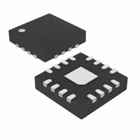
MAX8598ETE+ Maxim Integrated Products, MAX8598ETE+ Datasheet - Page 18

MAX8598ETE+
Manufacturer Part Number
MAX8598ETE+
Description
IC CNTRLR STP DWN LDO 16-TQFN
Manufacturer
Maxim Integrated Products
Datasheet
1.MAX8597ETP.pdf
(24 pages)
Specifications of MAX8598ETE+
Pwm Type
Controller
Number Of Outputs
1
Frequency - Max
1.4MHz
Duty Cycle
99.5%
Voltage - Supply
4.5 V ~ 28 V
Buck
Yes
Boost
No
Flyback
No
Inverting
No
Doubler
No
Divider
No
Cuk
No
Isolated
No
Operating Temperature
-40°C ~ 85°C
Package / Case
16-TQFN Exposed Pad
Frequency-max
1.4MHz
Lead Free Status / RoHS Status
Lead free / RoHS Compliant
where R
on-resistance (1.25Ω typ) and R
gate resistance of the MOSFET (typically 0.5Ω to 2Ω):
where V
In addition to the losses above, add approximately
20% more for additional losses due to MOSFET output
capacitances and low-side MOSFET body-diode
reverse-recovery charge dissipated in the high-side
MOSFET that exists, but is not well defined in the
MOSFET data sheet. Refer to the MOSFET data sheet
for thermal-resistance specification to calculate the
PC board area needed to maintain the desired maxi-
mum operating junction temperature with the above-
calculated power dissipation. To reduce EMI caused
by switching noise, add a 0.1µF or larger ceramic
capacitor from the high-side switch drain to the low-
side switch source or add resistors in series with DH
and DL to slow down the switching transitions.
However, adding a series resistor increases the power
dissipation of the MOSFETs, so be sure this does not
overheat the MOSFETs. The minimum load current must
exceed the high-side MOSFET’s maximum leakage plus
the maximum LX bias current over temperature.
The MAX8597/MAX8598/MAX8599 controllers sense
the peak inductor current to provide constant-current
and hiccup current limit. The peak current-limit thresh-
old is set by an external resistor (R2 in Figure 1) togeth-
er with the internal current sink of 200µA. The voltage
drop across the resistor R2 due to the 200µA current
sets the maximum peak inductor current that can flow
through the high-side MOSFET or the optional current-
sense resistor (between the high-side MOSFET source
and LX) by the equations below:
The actual corresponding maximum load current is
lower than the I
current. If the R
for current sensing, use the maximum R
highest operating junction temperature to avoid false
tripping of the current limit at elevated temperature.
Consideration should also be given to the tolerance of
the 200µA current sink. When the R
side MOSFET is used for current sensing, ringing on
Low-Dropout, Wide-Input-Voltage,
Step-Down Controllers
18
P
HSDR
______________________________________________________________________________________
I
PEAK(MAX)
GS
DH
= Q
I
PEAK(MAX)
~ V
is the high-side MOSFET driver’s average
gs
VL
DS(ON)
PEAK(MAX)
x V
= 5V.
= 200µA x R2 / R
GS
= 200µA x R2 / R
of the high-side MOSFET is used
x f
Setting the Current-Limit
S
by half of the inductor ripple
x R
GATE
GATE
DSON(HSFET)
DS(ON)
/ (R
SENSE
GATE
is the internal
DS(ON)
of the high-
+ R
DH
at the
)
the LX voltage waveform can interfere with the current
limit. Below is the procedure for selecting the value of the
series RC snubber circuit (R14 and C14 in Figure 1):
1) Connect a scope probe to measure V
2) Find the capacitor value (connected from LX to
The resistor for critical dampening (R14) is equal to 2π x
f
the desired damping and the peak voltage excursion.
The capacitor (C14) should be at least 2 to 4 times the
value of the C
loss of the snubber circuit is dissipated in the resistor
(R14) and is calculated as:
where V
frequency. Choose an R14 power rating that meets the
specific application’s derating rule for the power dissi-
pation calculated.
Additionally, there is parasitic inductance of the cur-
rent-sensing element, whether the high-side MOSFET
(L
(L
filter inductor. This parasitic inductance, together with
the output inductor, forms an inductive divider and
causes error in the current-sensing voltage. To com-
pensate for this error, a series RC circuit can be added
in parallel with the sensing element (see Figure 5). The
RC time constant should equal L
L
less than R2 / 100. Then, the value of C is calculated as:
Any PC board trace inductance in series with the sens-
ing element and output inductor should be added to
the specified FET or resistor inductance per the
respective manufacturer’s data sheet. For the case of
R
SENSE_FET
RSENSE
SENSE_FET
x L
and observe the ringing frequency, f
GND) that reduces the ringing frequency by half.
The circuit parasitic capacitance (C
then equal to 1/3 the value of the added capaci-
tance above. The circuit parasitic inductance (L
is calculated by:
PAR
IN
) are used, which is in series with the output
. Adjust the resistor value up or down to tailor
is the input voltage and f
/ R
C = L
C = L
L
) or the optional current-sense resistor
PAR
PAR
DS(ON)
P
R14
SENSE_FET
RSENSE
=
in order to be effective. The power
= C14 x (V
. First, set the value of R equal to or
(
2
π
×
/ (R
f
R
/ (R
)
1
2
SENSE
×
IN
DS(ON)
C
)
PAR
RSENSE
2
x f
x R) or
S
S
R
is the switching
x R)
.
PAR
/ R
LX
) at LX is
SENSE
to GND,
PAR
, or
)


