AD581LH Analog Devices Inc, AD581LH Datasheet - Page 9
AD581LH
Manufacturer Part Number
AD581LH
Description
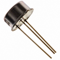
IC PREC VOLT REF 10V TO-5-3
Manufacturer
Analog Devices Inc
Datasheet
1.AD581LH.pdf
(12 pages)
Specifications of AD581LH
Temperature Coefficient
5ppm/°C
Reference Type
Series
Voltage - Output
10V
Tolerance
±5mV
Voltage - Input
12 ~ 30 V
Number Of Channels
1
Current - Quiescent
1mA
Current - Output
10mA
Operating Temperature
0°C ~ 70°C
Mounting Type
Through Hole
Package / Case
TO-5-3, Metal Can
Topology
Series
Input Voltage
12V To 30V
Reference Voltage
10V
Reference Voltage Tolerance
5mV
No. Of Pins
3
Operating Temperature Range
0°C To +70°C
Fixed / Adjust / Prog
Precision
Output Voltage (max)
10V
Reference Voltage Accuracy (max)
5
Line Regulation
0.005%/V
Load Regulation
500uV/mA
Input Voltage (max)
40V
Operating Temp Range
0C to 70C
Operating Temperature Classification
Commercial
Mounting
Through Hole
Pin Count
3
Package Type
TO-5
Lead Free Status / RoHS Status
Lead free / RoHS Compliant
Current - Cathode
-
Lead Free Status / Rohs Status
Compliant
Available stocks
Company
Part Number
Manufacturer
Quantity
Price
Company:

Part Number:
AD581LH
Manufacturer:
Analog Devices Inc
Quantity:
135


THE AD581 AS A CURRENT LIMITER
The AD581 represents an alternative to current limiter diodes
that require factory selection to achieve a desired current. This
approach often results in temperature coefficients of 1%/°C.
The AD581 approach is not limited to a defined set current
limit; it can be programmed from 0.75 mA to 5 mA with the
insertion of a single external resistor. Of course, the minimum
voltage required to drive the connection is 13 V. The AD580,
which is a 2.5 V reference, can be used in this type of circuit
with compliance voltage down to 4.5 V.
NEGATIVE 10 V REFERENCE
The AD581 can also be used in a 2-pin Zener mode to provide a
precision −10.00 V reference. As shown in Figure 13, the +V
V
case, ground). The ground pin is connected through a resistor
to the negative supply. Thus, the output is taken from the
ground pin instead of V
AD581 in this mode, a typical unit shows a 2 mV increase in
output level over that produced in the 3-pin mode. Note also
that the effective output impedance in this connection increases
from 0.2 Ω typical to 2 Ω. It is essential to arrange the output
load and the supply resistor, R
the AD581 is always between 1 mA and 5 mA. For operation to
+125°C, the net current should be between 2 mA and 5 mA. The
temperature characteristics and long-term stability of the device
are essentially the same as that of a unit used in the standard
3-pin mode.
The AD581 can also be used in a 2-pin mode to develop a
positive reference. +V
positive supply through an appropriate supply resistor. The
performance characteristics are similar to those of the negative
2-pin connection. The only advantage of this connection over
the standard 3-pin connection is that a lower primary supply
can be used, as low as 10.5 V. This type of operation requires con-
siderable attention to load and primary supply regulation to
maintain the AD581 within its regulating range of 1 mA to 5 mA
(2 mA to 5 mA for operation beyond +85°C).
OUT
pins are connected together to the high supply (in this
AD581
BOTTOM VIEW OF
10V PRECISION
REFERENCE CIRCUIT
IN TO-5 CASE
Figure 12. A Two-Component Precision Current Limiter
GND
+V
S
and V
OUT
S
V
OUT
. With 1 mA flowing through the
OUT
S
, so that the net current through
are tied together and to the
R
LOAD
10V =
i =
~ ___ + 0.75mA
10V
R
S
and
Rev. C | Page 9 of 12
10 V REFERENCE WITH MULTIPLYING CMOS DACs
OR ADCs
The AD581 is ideal for application with the entire
series of 10- and 12-bit multiplying CMOS DACs, especially for
low power applications. It is equally suitable for the
8-bit ADC. In the standard hook-up, as shown in Figure 15, the
+10 V reference is inverted by the amplifier/DAC configuration
to produce a 0 V to −10 V range. If an OP1177 amplifier is used,
total quiescent supply current is typically 2 mA. If a 0 V to +10 V
full-scale range is desired, the AD581 can be connected to the
CMOS DAC in its −10 V Zener mode, as shown in Figure 13
(the −10 V
CMOS DAC). The AD581 is normally used in the −10 V mode
with the AD7574 to give a 0 V to +10 V ADC range. This is
shown in Figure 15. Bipolar output applications and other
operating details can be found in the data sheets for the CMOS
products.
PRECISION 12-BIT DAC REFERENCE
AD565A, like most DACs, is designed to operate with a +10 V
reference element. In the AD565A, this 10 V reference voltage is
converted into a reference current of approximately 0.5 mA via
the internal 19.95 kΩ resistor (in series with the external 100 Ω
trimmer). The gain temperature coefficient of the AD565A is
primarily governed by the temperature tracking of the 19.95 kΩ
resistor and the 5 kΩ to10 kΩ span resistors; gain TC is guaran-
teed to 3 ppm/°C. Thus, using the AD581L (at 5 ppm/°C) as the
DIGITAL
INPUT
AD581
BIT 10 (LSB)
BIT 1 (MSB)
Figure 14. Low Power 10-Bit CMOS DAC Application
REF
0.1µF
output is connected directly to the V
V
+10V
Figure 13. 2-Pin −10 V Reference
REF IN
4
5
13
15
AD581
–15V
3
GND
+15V
+V
GND
1.2kΩ 5%
14
S
16
V
1
2
OUT
R
I
I
OUT1
OUT2
FEEDBACK
ANALOG
GND
–10V
V
REF
+15V
–15V
AD7533
REF IN
AD7574
0V TO –10V
AD581
of the
V
OUT
Related parts for AD581LH
Image
Part Number
Description
Manufacturer
Datasheet
Request
R

Part Number:
Description:
±1.7g Dual-Axis IMEMS Accelerometer Evaluation Board
Manufacturer:
Analog Devices Inc
Datasheet:

Part Number:
Description:
Inertial Sensor Evaluation System
Manufacturer:
Analog Devices Inc
Datasheet:
Part Number:
Description:
Manufacturer:
Analog Devices Inc
Datasheet:
Part Number:
Description:
Manufacturer:
Analog Devices Inc
Datasheet:
Part Number:
Description:
Manufacturer:
Analog Devices Inc
Datasheet:
Part Number:
Description:
Manufacturer:
Analog Devices Inc
Datasheet:
Part Number:
Description:
Manufacturer:
Analog Devices Inc
Datasheet:
Part Number:
Description:
Manufacturer:
Analog Devices Inc
Datasheet:
Part Number:
Description:
Manufacturer:
Analog Devices Inc
Datasheet:
Part Number:
Description:
Manufacturer:
Analog Devices Inc
Datasheet:
Part Number:
Description:
Manufacturer:
Analog Devices Inc
Datasheet:
Part Number:
Description:
Manufacturer:
Analog Devices Inc
Datasheet:
Part Number:
Description:
Manufacturer:
Analog Devices Inc
Datasheet: