AD581LH Analog Devices Inc, AD581LH Datasheet - Page 6
AD581LH
Manufacturer Part Number
AD581LH
Description
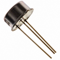
IC PREC VOLT REF 10V TO-5-3
Manufacturer
Analog Devices Inc
Datasheet
1.AD581LH.pdf
(12 pages)
Specifications of AD581LH
Temperature Coefficient
5ppm/°C
Reference Type
Series
Voltage - Output
10V
Tolerance
±5mV
Voltage - Input
12 ~ 30 V
Number Of Channels
1
Current - Quiescent
1mA
Current - Output
10mA
Operating Temperature
0°C ~ 70°C
Mounting Type
Through Hole
Package / Case
TO-5-3, Metal Can
Topology
Series
Input Voltage
12V To 30V
Reference Voltage
10V
Reference Voltage Tolerance
5mV
No. Of Pins
3
Operating Temperature Range
0°C To +70°C
Fixed / Adjust / Prog
Precision
Output Voltage (max)
10V
Reference Voltage Accuracy (max)
5
Line Regulation
0.005%/V
Load Regulation
500uV/mA
Input Voltage (max)
40V
Operating Temp Range
0C to 70C
Operating Temperature Classification
Commercial
Mounting
Through Hole
Pin Count
3
Package Type
TO-5
Lead Free Status / RoHS Status
Lead free / RoHS Compliant
Current - Cathode
-
Lead Free Status / Rohs Status
Compliant
Available stocks
Company
Part Number
Manufacturer
Quantity
Price
Company:

Part Number:
AD581LH
Manufacturer:
Analog Devices Inc
Quantity:
135


AD581
APPLYING THE AD581
The AD581 is easy to use in virtually all precision reference
applications. The three pins are simply: primary supply, ground,
and output, with the case grounded. No external components
are required even for high precision applications; the degree of
desired absolute accuracy is achieved simply by selecting the
required device grade. The AD581 requires less than 1 mA quies-
cent current from an operating supply range of 13 V to 30 V.
An external fine trim may be desired to set the output level to
exactly 10.000 V within less than a millivolt (calibrated to a
main system reference). System calibration may also require a
reference slightly different from 10.00 V. In either case, the
optional trim circuit shown in Figure 3 can offset the output by
up to ±30 mV (with the 22 Ω resistor), if needed, with minimal
effect on other device characteristics.
3.9Ω
22Ω
12Ω
R
RANGE
±30mV
±10mV
±5mV
TRIM
Figure 3. Optional Fine Trim Configuration
Figure 2. Pin Configuration (Bottom View)
–15V
3.5ppm/°C
2.0ppm/°C
0.6ppm/°C
Δ TCR
AD581
MAX
13V TO 30V
4.3kΩ
GND
6.8kΩ
+V
10kΩ
S
V
OUT
AD581
10V
+15V
GND
+V
S
R
V
OUT
+10V
Rev. C | Page 6 of 12
VOLTAGE VARIATION vs. TEMPERATURE
Some confusion exists in the area of defining and specifying
reference voltage error over temperature. Historically, references
have been characterized using a maximum deviation per degree
Celsius; that is, 10 ppm/°C. However, because of nonlinearities
in temperature characteristics, which originated in standard
Zener references (such as S-type characteristics) manufacturers
opt for the maximum limit error band approach to specify devices.
This technique involves measurement of the output at three,
five, or more different temperatures to guarantee that the output
voltage falls within the given error band. The temperature charac-
teristic of the AD581 consistently follows the S-curve shown in
Figure 5. Three-point measurement of each device guarantees
the error band over the specified temperature range.
Q10
Q3
Q16
R40
10.005
10.000
9.995
R39
–55
Q4
–50
C51
Figure 5. Typical Temperature Characteristic
–40 –30 –20 –10 0
C52
Q6
Figure 4. Simplified Schematic
Q13
C50
Q12
TEMPERATURE (°C)
10 20 30 40 50 60 70 80 90 100 110 120 125
Q11
Q14
R41
Q20
Q2
R33
R30
Q15
Q8
Q1
R31
Q5
R32
Q7
R42
R34
R37
R35
R36
10V
V+
V–
Related parts for AD581LH
Image
Part Number
Description
Manufacturer
Datasheet
Request
R

Part Number:
Description:
±1.7g Dual-Axis IMEMS Accelerometer Evaluation Board
Manufacturer:
Analog Devices Inc
Datasheet:

Part Number:
Description:
Inertial Sensor Evaluation System
Manufacturer:
Analog Devices Inc
Datasheet:
Part Number:
Description:
Manufacturer:
Analog Devices Inc
Datasheet:
Part Number:
Description:
Manufacturer:
Analog Devices Inc
Datasheet:
Part Number:
Description:
Manufacturer:
Analog Devices Inc
Datasheet:
Part Number:
Description:
Manufacturer:
Analog Devices Inc
Datasheet:
Part Number:
Description:
Manufacturer:
Analog Devices Inc
Datasheet:
Part Number:
Description:
Manufacturer:
Analog Devices Inc
Datasheet:
Part Number:
Description:
Manufacturer:
Analog Devices Inc
Datasheet:
Part Number:
Description:
Manufacturer:
Analog Devices Inc
Datasheet:
Part Number:
Description:
Manufacturer:
Analog Devices Inc
Datasheet:
Part Number:
Description:
Manufacturer:
Analog Devices Inc
Datasheet:
Part Number:
Description:
Manufacturer:
Analog Devices Inc
Datasheet: