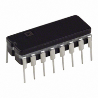
AD652AQ Analog Devices Inc, AD652AQ Datasheet - Page 15

AD652AQ
Manufacturer Part Number
AD652AQ
Description
IV V-F CONVERTER SYNC 16-CDIP
Manufacturer
Analog Devices Inc
Type
Voltage to Frequencyr
Specifications of AD652AQ
Rohs Status
RoHS non-compliant
Frequency - Max
2MHz
Full Scale
±50ppm/°C
Linearity
±0.02%
Mounting Type
Through Hole
Package / Case
16-CDIP (0.300", 7.62mm)
Full Scale Range
1MHz To 2MHz
Linearity %
0.02%
Supply Voltage Range
± 6V To ± 18V
Digital Ic Case Style
DIP
No. Of Pins
16
Frequency Max
2MHz
Termination Type
Through Hole
Converter Function
VFC
Full Scale Frequency
2000
Power Supply Requirement
Single/Dual
Single Supply Voltage (max)
36V
Single Supply Voltage (min)
12V
Dual Supply Voltage (typ)
±15V
Dual Supply Voltage (min)
±6V
Dual Supply Voltage (max)
±18V
Operating Temperature (min)
-40C
Operating Temperature (max)
85C
Operating Temperature Classification
Industrial
Package Type
CDIP
Converter Type
Voltage to Frequency
Current, Quiescent Supply
±11 mA (Typ.)
Frequency Range
5 MHz (Typ.)
Input Impedance
20 Kiloohms
Number Of Pins
20
Temperature, Operating, Maximum
85 °C
Temperature, Operating, Minimum
-40 °C
Voltage, Range
±6 to ±18 V
Voltage, Supply
36 V
Filter Terminals
Through Hole
Rohs Compliant
No
Calibration Error Fs Typ
5%
Lead Free Status / Rohs Status
Not Compliant
Available stocks
Company
Part Number
Manufacturer
Quantity
Price
Company:
Part Number:
AD652AQ
Manufacturer:
TOSHIBA
Quantity:
670
FREQUENCY-TO-VOLTAGE CONVERTER
The AD652 SVFC also works as a frequency-to-voltage
converter. Figure 22 shows the connection diagram for F/V
conversion. In this case, the negative input of the comparator is
fed the input pulses. Either comparator input may be used so
that an input pulse of either polarity may be applied to the F/V.
In Figure 22, the + input is tied to a 1.2 V reference and low-
level TTL pulses are used as the frequency input. The pulse
must be low on the falling edge of the clock. On the subsequent
rising edge, the 1 mA current source is switched to the
integrator summing junction and ramps up the voltage at Pin 4.
Due to the action of the AND gate, the 1 mA current is switched
off after only one clock period. The average current delivered to
the summing junction varies from 0 mA to 0.5 mA; using the
internal 20 kΩ resistor, this results in a full-scale output voltage
of 10 V at Pin 4.
The frequency response of the circuit is determined by the
capacitor; the −3 dB frequency is simply the RC time constant.
A tradeoff exists between ripple and response. If low ripple is
desired, a large value capacitor must be used (1 µF); if fast
response is needed, a small capacitor is used (1 nF minimum).
The op amp can drive a 5 kΩ resistor load to 10 V, using a 15 V
positive power supply. If a large load capacitance (0.01 µF) must
be driven, it is necessary to isolate the load with a 50 Ω resistor
V
OUT
+
–
5kΩ
0.01µF
50Ω
CLOCK
VOLTS
FREQ
+V
–V
C
OUT
Figure 22. Frequency-to-Voltage Converter
S
S
IN
1
2
3
4
5
6
7
8
20kΩ
LOADS ON FALLING EDGE OF CK
SHIFTS OUT ON RISING EDGE OF CL
FREQUENCY TO VOLTS CONVERTER
SYNCHRONOUS
VOLTAGE-TO-
FREQUENCY
CONVERTER
AD652
Rev. C | Page 15 of 28
1mA
REFERENCE
as shown. Because the 50 Ω resistor is 0.25% of the full scale,
and the specified gain error with the 20 kΩ resistor is 0.5%, this
extra resistor only increases the total gain error to 0.75% max.
The circuit shown is unipolar and only a 0 V to +10 V output is
allowed. The integrator op amp is not a general-purpose op
amp. Instead, it has been optimized for simplicity and high
speed. The most significant difference between this amplifier
and a general-purpose op amp is the lack of an integrator (or
level shift) stage.
Consequently, the voltage on the output (Pin 4) must always be
more positive than 1 V below the inputs (Pins 6 and 7). For
example, in the F-to-V conversion mode, the noninverting input
of the op amp (Pin 6) is grounded, which means the output
(Pin 4) cannot go below −1 V. Normal operation of the circuit as
shown never calls for a negative voltage at the output.
A second difference between this op amp and a general-purpose
amplifier is that the output only sinks 1.5 mA to the negative
supply. The only pull-down other than the 1 mA current used
for voltage-to-frequency conversion is a 0.5 mA source. The op
amp sources a great deal of current from the positive supply,
and is internally protected by current limiting. The op amp
output may be driven to within 4 V of the positive supply when
not sourcing external current. When sourcing 10 mA, the out-
put voltage may be driven to within 6 V of the positive supply.
AND
5V
D
SHOT
ONE
Q
Q
FLOP
"D"
CK
16
15
14
13
12
11
10
9
FREQ
NC
NC
IN
5V
CLOCK
5kΩ
1N4148
DIGITAL
GND
AD652


