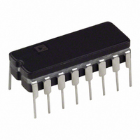
AD652BQ Analog Devices Inc, AD652BQ Datasheet - Page 23

AD652BQ
Manufacturer Part Number
AD652BQ
Description
IC V-F CONVERTER SYNC 16-CDIP
Manufacturer
Analog Devices Inc
Type
Voltage to Frequencyr
Datasheet
1.AD652JPZ.pdf
(28 pages)
Specifications of AD652BQ
Rohs Status
RoHS non-compliant
Frequency - Max
2MHz
Full Scale
±25ppm/°C
Linearity
±0.005%
Mounting Type
Through Hole
Package / Case
16-CDIP (0.300", 7.62mm)
Converter Function
VFC
Full Scale Frequency
2000
Power Supply Requirement
Single/Dual
Single Supply Voltage (max)
36V
Single Supply Voltage (min)
12V
Dual Supply Voltage (typ)
±15V
Dual Supply Voltage (min)
±6V
Dual Supply Voltage (max)
±18V
Operating Temperature (min)
-40C
Operating Temperature (max)
85C
Operating Temperature Classification
Industrial
Package Type
CDIP
Lead Free Status / Rohs Status
Not Compliant
Available stocks
Company
Part Number
Manufacturer
Quantity
Price
Part Number:
AD652BQ
Manufacturer:
ADI/亚德诺
Quantity:
20 000
DELTA MODULATOR
The circuit of Figure 34 shows the AD652 configured as a delta
modulator. A reference voltage is applied to the input of the
integrator (Pin 7), which sets the steady state output frequency
at one-half of the AD652 full-scale frequency (1/4 of the clock
frequency). As a 0 V to 10 V input signal is applied to the
comparator (Pin 15), the output of the integrator attempts to
track this signal. For an input in an idling condition (dc), the
output frequency is one-half full scale. For positive-going
signals, the output frequency is between one-half full scale and
full scale; for negative-going signals, the output frequency is
between zero and one-half full scale. The output frequency
corresponds to the slope of the comparator input signal.
–15V
Since the output frequency corresponds to the slope of the input
signal, the delta modulator acts as a differentiator. A delta
modulator is thus a direct way of finding the derivative of a
signal. This is useful in systems where, for example, a signal
corresponding to velocity exists, and it is desired to determine
acceleration.
Figure 35 is a scope photo showing a 20 kHz, 0 V to 10 V sine
wave used as the input to the comparator and its ramp-wise
approximation at the integrator output. The clock frequency
used as 2 MHz and the integrating capacitor was 360 pF.
Figure 36 shows the same input signal and its ramp-wise
approximation, along with the output frequency corresponding
to the derivative of the input signal. In this case, the clock
frequency was 50 kHz.
+15V
360pF
1
2
3
4
5
6
7
8
20kΩ
SYNCHRONOUS
VOLTAGE-TO-
FREQUENCY
CONVERTER
AD652
1mA
Figure 34. Delta Modulator
0.0047µF
REFERENCE
AND
5V
D
SHOT
ONE
Q
Q
FLOP
"D"
CK
16
15
14
13
12
11
10
9
0.01µF
CLOCK
+5V
V
IN
1kΩ
(0V TO 10V)
F
Rev. C | Page 23 of 28
OUT
The choice of an integrating capacitor is primarily dictated by
the input signal bandwidth. Figure 37 shows this relationship.
Note that as the value of C
integrator approximation becomes larger. This can be
compensated for by increasing the clock frequency. The effect of
the clock frequency on the ramp size is demonstrated in
Figure 35 and Figure 36.
Figure 35. Delta Modulator Input Signal and Ramp-Wise Approximation
Figure 36. Delta Modulator Input Signal Ramp-Wise Approximation and
Figure 37. Maximum Integrating Cap Value vs. Input Signal Bandwidth
10k
100
1k
100
INPUT SIGNAL BANDWIDTH (Hz)
Output Frequency
1k
INT
is lowered, the ramp size of the
10k
AD652


