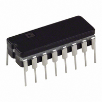
AD652BQ Analog Devices Inc, AD652BQ Datasheet - Page 10

AD652BQ
Manufacturer Part Number
AD652BQ
Description
IC V-F CONVERTER SYNC 16-CDIP
Manufacturer
Analog Devices Inc
Type
Voltage to Frequencyr
Datasheet
1.AD652JPZ.pdf
(28 pages)
Specifications of AD652BQ
Rohs Status
RoHS non-compliant
Frequency - Max
2MHz
Full Scale
±25ppm/°C
Linearity
±0.005%
Mounting Type
Through Hole
Package / Case
16-CDIP (0.300", 7.62mm)
Converter Function
VFC
Full Scale Frequency
2000
Power Supply Requirement
Single/Dual
Single Supply Voltage (max)
36V
Single Supply Voltage (min)
12V
Dual Supply Voltage (typ)
±15V
Dual Supply Voltage (min)
±6V
Dual Supply Voltage (max)
±18V
Operating Temperature (min)
-40C
Operating Temperature (max)
85C
Operating Temperature Classification
Industrial
Package Type
CDIP
Lead Free Status / Rohs Status
Not Compliant
Available stocks
Company
Part Number
Manufacturer
Quantity
Price
Part Number:
AD652BQ
Manufacturer:
ADI/亚德诺
Quantity:
20 000
AD652
SVFC CONNECTION FOR BIPOLAR INPUT VOLTAGES
A bipolar input voltage of ±5 V can be accommodated by
injecting a 250 µA current into Pin 5 (see Figure 10). A −5 V
signal provides a zero sum current at the integrator summing
junction, which results in a zero-output frequency; a +5 V signal
provides a 0.5 mA (full-scale) sum current, which results in the
full-scale output frequency.
Using an external resistor to inject the offset current has some
effect on the bipolar offset temperature coefficient. The ideal
transfer curve with bipolar inputs is shown in Figure 11. The
user actually has four options to use in injecting the bipolar
offset current into the inverting input of the op amp:
1.
2.
3.
4.
Option 4 provides the closest to the ideal transfer function as
diagrammed in Figure 11. Figure 12 shows the effects of the
transfer relation on the other three options. In the first case, the
slope of the transfer function is unchanged with temperature.
However, V
frequency of 0 Hz) and F
V
to the voltage axis with temperature. In the second case, F
remains constant, but V
rotates about F
with two external resistors, the V
while the slope and offset of the transfer function change with
temperature. If selecting this third option, the user should select
low drift, matched resistors.
IN
= 0 V) changes as the transfer function is displaced parallel
Use an external resistor for R
resistor for R
Use the internal 20 kΩ resistor as R
Use two external resistors.
Use two internal resistors for R
PLCC version only).
ZERO
ZERO
(the input voltage required to produce an output
IN
with temperature changes. In the third case,
(as shown in Figure 10).
ZERO
ZERO
changes as the transfer function
(the output frequency when
±5V
V
IN
ZERO
OS
20kΩ
C
IN
INT
and the internal 20 kΩ
point remains invariant
and R
–V
OS
+V
S
and an external R
S
OS
1
2
3
4
5
6
7
8
(available on
20kΩ
SYNCHRONOUS
VOLTAGE-TO-
FREQUENCY
CONVERTER
AD652
1mA
ZERO
Figure 10. Bipolar Offset
IN
Rev. C | Page 10 of 28
.
REFERENCE
AND
5V
D
SHOT
ONE
Q
Q
FLOP
"D"
V
CASE 1
R
R
CASE 2
R
R
CASE 3
R
R
CK
IN
IN
OS
IN
OS
IN
OS
∼
∼
∼
∼
∼
∼
R
INTERNAL
EXTERNAL
EXTERNAL
IN
EXTERNAL
INTERNAL
EXTERNAL
V
Figure 11. Ideal Bipolar Input Transfer Curve over Temperature
16
15
14
13
12
11
10
9
REF
V
Figure 12. Actual Bipolar Input Transfer over Temperature
R
ZERO
OS
R
ANALOG
GND
L
C
–5V
–5V
–5V
OS
CLOCK
IDEAL
IDEAL
5V
V
ZERO
V
ZERO
V
ZERO
DIGITAL
GND
FREQ
OUT
IDEAL
F
F
F
TRANSFER
RELATION
–5V
OUT
OUT
OUT
IDEAL
F
F
F
ZERO
ZERO
ZERO
TEMPERATURE
PERTURBED
TRANSFER
TEMPERATURE
PERTURBED
TEMPERATURE
PERTURBED
F
OUT
F
ZERO
+5V
V
V
V
IN
IN
IN
V
IN


