AD537JH Analog Devices Inc, AD537JH Datasheet - Page 6
AD537JH
Manufacturer Part Number
AD537JH
Description
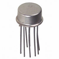
IC V/F CONV TO-100-10
Manufacturer
Analog Devices Inc
Type
Voltage to Frequencyr
Specifications of AD537JH
Rohs Status
RoHS non-compliant
Frequency - Max
100kHz
Full Scale
±30ppm/°C
Linearity
±0.05%
Mounting Type
Through Hole
Package / Case
TO-100-10 Metal Can
Frequency
150kHz
Full Scale Range
0kHz To 150kHz
Linearity %
0.15%
Supply Voltage Range
4.5V To 36V
Digital Ic Case Style
TO-100
No. Of Pins
10
Msl
MSL 1 - Unlimited
Converter Function
VFC
Full Scale Frequency
150
Power Supply Requirement
Single/Dual
Single Supply Voltage (typ)
5/9/12/15/18/24/28V
Single Supply Voltage (max)
36V
Single Supply Voltage (min)
4.5V
Dual Supply Voltage (typ)
±9/±12/±15V
Dual Supply Voltage (min)
±5V
Dual Supply Voltage (max)
±18V
Operating Temperature (min)
0C
Operating Temperature (max)
70C
Operating Temperature Classification
Commercial
Package Type
TO-100
Converter Type
Voltage to Frequency
Current, Quiescent Supply
1.2 μA
Frequency Range
0 to 150 kHz
Number Of Pins
10
Temperature, Operating, Maximum
70 °C
Temperature, Operating, Minimum
0 °C
Voltage, Range
1 V (Min.)
Voltage, Supply
5 to 36 V
Low Power
1.2 mA quiescent current
Lead Free Status / Rohs Status
Not Compliant
Available stocks
Company
Part Number
Manufacturer
Quantity
Price

Part Number:
AD537JH
Manufacturer:
ADI/亚德诺
Quantity:
20 000


AD537
F-V CONVERTERS
The AD537 can be used as a high linearity VCO in a phase-
locked loop to accomplish frequency-to-voltage conversion. By
operating the loop without a low-pass filter in the feedback path
(first-order system), it can lock to any frequency from zero to an
upper limit determined by the design, responding in three or
four cycles to a step change of input frequency. In practice, the
overall response time is determined by the characteristics of the
averaging filter which follows the PLL.
Figure 7 shows a connection using a low power TTL quad
open-collector nand gate which serves as the phase comparator.
The input signal should be a pulse train or square wave with
characteristics similar to TTL or 5-volt CMOS outputs. Any
duty cycle is acceptable, but the minimum pulse width is 40 µs.
The output voltage is one volt for a 10 kHz input frequency.
The output as shown here is at a fairly high impedance level; for
many situations an additional buffer may be required.
Trimming is similar to V-F application trimming. First set the
V
trim the 2 kΩ potentiometer for 1.00 volts out. Then apply a
10 Hz waveform and trim the V
the full-scale output at 10 kHz. Other frequency scales can be
obtained by appropriate scaling of timing components.
TEMPERATURE-TO-FREQUENCY CONVERSION
The linear temperature-proportional output of the AD537 can
be used as shown in these applications to perform various direct
temperature-to-frequency conversion functions; it can also be
used with other external connections in a temperature sensing
or compensation scheme. If the sensor output is used externally,
it should be buffered through an op amp since loading that
point will cause significant error in the sensor output as well as
in the main V-F converter circuitry.
An absolute temperature (Kelvin)-to-frequency converter is very
easily accomplished, as shown in Figure 8. The 1 mV per K out-
put serves as the input to the buffer amplifier, which then scales
the oscillator drive current to a nominal 298 µA at +25°C
(298K). Use of a 1000 pF capacitor results in a corresponding
frequency of 2.98 kHz. Setting the single 2 kΩ trimmer for the
correct frequency at a well-defined temperature near +25°C will
9.09k
OS
2k
trimmer to mid-scale. Apply a 10 kHz input frequency and
0.005µF
1
2
3
4
5
6
7
REFERENCE
BUF
PRECISION
Figure 7. 10 kHz F-V Converter
VOLTAGE
3.9k
AD537
DRIVER
CURR
FREQ
CONV
-TO-
120k
0.33µF
14
13
12
11
10
9
8
1N4148
(0-10kHz)
OUTPUT
1V F.S.
0.001µF
f
IN
10k
20k
V
OS
OS
for 1 mV out. Finally, retrim
+5V
10k
10k
74LO3
10k
–6–
normally result in an accuracy of ± 2°C from –55°C to +125°C
(using an AD537S). An NPO ceramic capacitor is recom-
mended to minimize nonlinearity due to capacitance drift.
OFFSET TEMPERATURE SCALES
Many other temperature scales can be set up by offsetting the
temperature output with the voltage reference output. Such a
scheme is shown by the Celsius-to-frequency converter in
Figure 9. Corresponding component values for a Fahrenheit-to-
frequency converter which give 10 Hz/°F are given in parentheses.
Figure 9. Offset Temperature Scale Converters Centigrade
and (Fahrenheit) to Frequency
A simple calibration procedure which will provide ± 2°C accu-
racy requires substitution of a 7.27k resistor for the series com-
bination of the 6.04k with the 2k trimmer; then simply set the
500 Ω trimmer to give 250 Hz at +25°C.
High accuracy calibration procedure:
1. Measure room temperature in K.
2. Measure temperature output at Pin 6 at that temperature.
3. Calculate offset adjustment as follows:
4. Temporarily disconnect 49 Ω resistor (or 500 Ω pot) and
5. Adjust slope trimmer to give proper frequency at room tem-
Figure 8. Absolute Temperature to Frequency Converter
trim 2 kΩ pot to give the offset voltage at the indicated node.
Reconnect 49 Ω resistor.
perature (+25°C = 250 Hz).
Adjustment for °F or any other scale is analogous.
(4.02k)
Offset Voltage ( mV ) =
2.74k
500Ω
6.04k
(10k)
+V
(205Ω)
2kΩ
49Ω
V
TEMP
2k
9.1kΩ
2
3
V
REF
1
2
3
4
5
6
7
1
4
(CONNECTED TO CASE)
BUF
AD537
V
V
V
V
T
R
R
T
V
REFERENCE
BUF
PRECISION
TEMP
VOLTAGE
REFERENCE
PRECISION
–V
VOLTAGE
Room temp ( K )
10
TO-FREQ
5
DRIVER
CURR-
S
CONV
TO-FREQ
DRIVER
CURR-
CONV
AD537
( Pin 6 ) ( mV )
LOGIC
GND
9
6
14
13
12
11
10
9
8
8
7
10kΩ
1000pF
+V
10k
S
3900 pF
(1500pF)
f = 10Hz/K
× 273.2
f
10Hz/°C
(10Hz/°F)
+5V
OUT
REV. C
Related parts for AD537JH
Image
Part Number
Description
Manufacturer
Datasheet
Request
R

Part Number:
Description:
±1.7g Dual-Axis IMEMS Accelerometer Evaluation Board
Manufacturer:
Analog Devices Inc
Datasheet:

Part Number:
Description:
Inertial Sensor Evaluation System
Manufacturer:
Analog Devices Inc
Datasheet:
Part Number:
Description:
Manufacturer:
Analog Devices Inc
Datasheet:
Part Number:
Description:
Manufacturer:
Analog Devices Inc
Datasheet:
Part Number:
Description:
Manufacturer:
Analog Devices Inc
Datasheet:
Part Number:
Description:
Manufacturer:
Analog Devices Inc
Datasheet:
Part Number:
Description:
Manufacturer:
Analog Devices Inc
Datasheet:
Part Number:
Description:
Manufacturer:
Analog Devices Inc
Datasheet:
Part Number:
Description:
Manufacturer:
Analog Devices Inc
Datasheet:
Part Number:
Description:
Manufacturer:
Analog Devices Inc
Datasheet:
Part Number:
Description:
Manufacturer:
Analog Devices Inc
Datasheet:
Part Number:
Description:
Manufacturer:
Analog Devices Inc
Datasheet:
Part Number:
Description:
Manufacturer:
Analog Devices Inc
Datasheet: