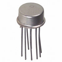
AD537JH Analog Devices Inc, AD537JH Datasheet

AD537JH
Specifications of AD537JH
Available stocks
Related parts for AD537JH
AD537JH Summary of contents
Page 1
...
Page 2
... Rated Performance Storage 6, 7 PACKAGE OPTIONS D-14 Ceramic DIP H-10A Header NOTES *Specifications same as AD537JH. **Specifications same as AD537K. 1 Nonlinearity is specified for a current input level (I IN reduced linearity. Nonlinearity is defined as deviation from a straight line from zero to full scale, expressed as a percentage of full scale. 2 Guaranteed not tested ...
Page 3
CIRCUIT OPERATION Block diagrams of the AD537 are shown above. A versatile operational amplifier (BUF) serves as the input stage; its pur- pose is to convert and scale the input voltage signal to a drive current in the NPN follower. ...
Page 4
AD537 In some cases the signal may be in the form of a negative cur- rent source. This can be handled in a similar way to a negative input voltage. However, the scaling resistor is no longer re- quired, eliminating ...
Page 5
NONLINEARITY SPECIFICATION The preferred method for specifying linearity error is in terms of the maximum deviation from the ideal relationship after cali- brating the converter at full scale and “zero”. This error will vary with the full-scale frequency and the ...
Page 6
AD537 F-V CONVERTERS The AD537 can be used as a high linearity VCO in a phase- locked loop to accomplish frequency-to-voltage conversion. By operating the loop without a low-pass filter in the feedback path (first-order system), it can lock to ...
Page 7
SYNCHRONOUS OPERATION The SYNC terminal at pin 2 of the DIP package can be used to synchronize a free running AD537 to a master oscillator, either at a multiple or a sub-multiple of the primary frequency. The preferred connection is ...
Page 8
AD537 THERMOCOUPLE INPUT The output of a Chromel-Constantan (Type E) thermocouple, using a reference junction at 0°C, varies from 53.14 mV over the temperature range 0°C to +700°C with a slope of 80.678 µV/degree over most of ...


