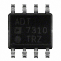
ADT7310TRZ Analog Devices Inc, ADT7310TRZ Datasheet - Page 4

ADT7310TRZ
Manufacturer Part Number
ADT7310TRZ
Description
IC TEMP SENSOR 16BIT SPI 8SOIC
Manufacturer
Analog Devices Inc
Datasheet
1.ADT7310TRZ.pdf
(24 pages)
Specifications of ADT7310TRZ
Function
Temp Monitoring System (Sensor)
Topology
ADC (Sigma Delta), Oscillator, Register Bank
Sensor Type
Internal
Sensing Temperature
-55°C ~ 150°C
Output Type
SPI™
Output Alarm
Yes
Output Fan
No
Voltage - Supply
2.7 V ~ 5.5 V
Operating Temperature
-55°C ~ 150°C
Mounting Type
Surface Mount
Package / Case
8-SOIC (3.9mm Width)
Ic Output Type
Digital
Sensing Accuracy Range
± 0.5°C
Supply Current
230µA
Supply Voltage Range
2.7V To 5.5V
Resolution (bits)
16bit
Sensor Case Style
SOIC
No. Of Pins
8
Temperature Sensor Function
Temp Sensor
Package Type
SOIC N
Operating Temperature (max)
150C
Operating Temperature Classification
Military
Operating Supply Voltage (min)
2.7V
Operating Supply Voltage (typ)
3.3/5V
Operating Supply Voltage (max)
5.5V
Lead Free Status / RoHS Status
Lead free / RoHS Compliant
Lead Free Status / RoHS Status
Lead free / RoHS Compliant, Lead free / RoHS Compliant
Available stocks
Company
Part Number
Manufacturer
Quantity
Price
Company:
Part Number:
ADT7310TRZ-REEL7
Manufacturer:
AD
Quantity:
2 100
ADT7310
SPI TIMING SPECIFICATIONS
T
(10% to 90% of V
Table 2.
Parameter
t
t
t
t
t
t
t
t
t
t
1
2
3
4
1
2
3
4
5
6
7
8
9
10
Sample tested during initial release to ensure compliance. All input signals are specified with t
See Figure 2.
SCLK active edge is falling edge of SCLK.
This means that the times quoted in the timing characteristics are the true bus relinquish times of the part and, as such, are independent of external bus loading
capacitances.
A
4
= −55°C to +150°C, V
1, 2
DOUT
SCLK
DIN
CS
DD
) and timed from a voltage level of 1.6 V.
Limit at T
0
100
100
30
25
0
60
80
10
80
0
0
60
80
10
DD
= 2.7 V to 5.5 V, unless otherwise noted. All input signals are specified with rise time (t
t
t
9
1
MIN
t
4
MSB
, T
t
t
1
2
5
MAX
(B Version)
2
OUTPUT
t
3
Figure 3. Load Circuit for Timing Characterization
PIN
TO
3
Figure 2. Detailed SPI Timing Diagram
10pF
Rev. 0 | Page 4 of 24
Unit
ns min
ns min
ns min
ns min
ns min
ns min
ns max
ns max
ns min
ns max
ns min
ns min
ns max
ns max
ns min
I
100µA WITH V
I SOURCE
100µA WITH V
SINK
(1.6mA WITH V
(200µA WITH V
7
1.6V
Conditions/Comments
CS falling edge to SCLK active edge setup time
SCLK high pulse width
SCLK low pulse width
Data valid to SCLK edge setup time
Data valid to SCLK edge hold time
SCLK active edge to data valid delay
V
V
Bus relinquish time after CS inactive edge
CS rising edge to SCLK edge hold time
CS falling edge to DOUT active time
V
V
SCLK inactive edge to DOUT high
DD
DD
DD
DD
DD
DD
R
= 3V)
= 3V)
= t
LSB
= 4.5 V to 5.5 V
= 2.7 V to 3.6 V
= 4.5 V to 5.5 V
= 2.7 V to 3.6 V
DD
8
F
= 5 ns (10% to 90% of V
= 5V,
DD
MSB
= 5V,
1
t
6
2
DD
) and timed from a voltage level of 1.6 V.
7
LSB
t
t
8
10
8
3
R
t
7
) = fall time (t
3
F
) = 5 ns


