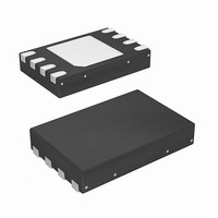
SE97BTP,547 NXP Semiconductors, SE97BTP,547 Datasheet - Page 6

SE97BTP,547
Manufacturer Part Number
SE97BTP,547
Description
IC TEMP SENSOR DIMM 8HWSON
Manufacturer
NXP Semiconductors
Datasheet
1.SE97BTP547.pdf
(53 pages)
Specifications of SE97BTP,547
Package / Case
8-WSON (Exposed Pad), 8-HWSON
Function
Temp Monitoring System (Sensor)
Topology
ADC (Sigma Delta), Comparator, Register Bank
Sensor Type
Internal
Sensing Temperature
-40°C ~ 125°C
Output Type
I²C™/SMBus™
Output Alarm
Yes
Output Fan
Yes
Voltage - Supply
3 V ~ 3.6 V
Operating Temperature
-40°C ~ 125°C
Mounting Type
Surface Mount
Temperature Threshold
+ 150 C
Full Temp Accuracy
2 C
Digital Output - Bus Interface
I2C
Digital Output - Number Of Bits
11 bit
Supply Voltage (max)
3.6 V
Supply Voltage (min)
3 V
Description/function
Temperature Sensor
Maximum Operating Temperature
+ 125 C
Minimum Operating Temperature
- 40 C
Lead Free Status / RoHS Status
Lead free / RoHS Compliant
Lead Free Status / RoHS Status
Lead free / RoHS Compliant, Lead free / RoHS Compliant
Other names
568-5055-2
NXP Semiconductors
7. Functional description
SE97B_1
Product data sheet
Fig 3.
MSB
0
a. Temperature sensor
0
fixed
Slave address
slave address
1
1
7.1 Serial bus interface
7.2 Slave address
A2
selectable
hardware
The SE97B communicates with a host controller by means of the 2-wire serial bus
(I
device supports SMBus, I
speed is defined to have bus speeds from 0 Hz to 100 kHz, I
to 400 kHz, and the SMBus is from 10 kHz to 100 kHz. The host or bus master generates
the SCL signal, and the SE97B uses the SCL signal to receive or send data on the SDA
line. Data transfer is serial, bidirectional, and is one byte at a time with the Most Significant
Bit (MSB) transferred first. Since SCL and SDA are open-drain, pull-up resistors must be
installed on these pins.
The SE97B uses a 4-bit fixed and 3-bit programmable (A0, A1 and A2) 7-bit slave address
that allows a total of eight devices to coexist on the same bus. The A0, A1 and A2 pins are
pulled LOW internally. The A0 pin is also overvoltage tolerant supporting 10 V software
write protect. When it is driven higher than 7.0 V, writing a special command would put the
EEPROM in reversible write protect mode (see
Each pin is sampled at the start of each I
sensor’s fixed address is ‘0011b’. The EEPROM’s fixed address for the normal EEPROM
read/write is ‘1010b’, and for EEPROM software protection command is ‘0110b’. Refer to
Figure
A1
2
C-bus/SMBus) that consists of a serial clock (SCL) and serial data (SDA) signals. The
LSB
002aab304
A0
3.
R/W
X
MSB
1
b. EEPROM (normal read/write)
Rev. 01 — 27 January 2010
0
fixed
2
C-bus Standard-mode and Fast-mode. The I
slave address
1
DDR memory module temp sensor with integrated SPD
0
A2
selectable
hardware
A1
2
LSB
C-bus/SMBus access. The temperature
002aab351
A0
R/W
X
Section 7.10.2 “Memory
MSB
0
c. EEPROM (software
2
1
C-bus fast speed from 0 Hz
fixed
protection command)
slave address
1
0
© NXP B.V. 2010. All rights reserved.
2
A2
C-bus standard
Protection”).
selectable
hardware
SE97B
A1
LSB
002aab352
A0
R/W
X
6 of 53


