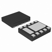
NCP362CMUTBG ON Semiconductor, NCP362CMUTBG Datasheet

NCP362CMUTBG
Specifications of NCP362CMUTBG
Available stocks
Related parts for NCP362CMUTBG
NCP362CMUTBG Summary of contents
Page 1
NCP362 USB Positive Overvoltage and Overcurrent Protection with TVS for V BUS Capacitance ESD Diodes for Data The NCP362 disconnects systems at its output when wrong VBUS operating conditions are detected at its input. The system is positive overvoltage protected ...
Page 2
USB Connector Bottom Connector VIN/VBUS VBUS Pin 1 Pin 2 D+ Pin 3 D− Pin 4 ID Pin 5 GND VBUS TVS Figure 1. Typical Application Circuit with Wall Adapter / V USB Connector VIN/VBUS VBUS Pin 1 D+ Pin ...
Page 3
PIN FUNCTION DESCRIPTION Pin No. Name Type 1 EN INPUT Enable Pin. The device enters in shutdown mode when this pin is tied to a high level. In this case the output is disconnected from the input. To allow normal ...
Page 4
MAXIMUM RATINGS Rating Minimum Voltage to GND (Pins IN, EN, OUT, FLAG) Maximum Voltage to GND (Pin IN) Maximum Voltage to GND (Pins EN, OUT, FLAG) Maximum DC Current from Vin to Vout (PMOS) (Note 1) Thermal Resistance, Junction−to−Air Operating ...
Page 5
ELECTRICAL CHARACTERISTICS (Min/Max limits values (−40°C < T < +85°C) and V A Characteristic Symbol Input Voltage Range Undervoltage Lockout Threshold UVLO Uvervoltage Lockout Hysteresis UVLO Overvoltage Lockout Threshold OVLO Overvoltage Lockout Hysteresis OVLO V versus V Dopout V in ...
Page 6
... Test Current T I Forward Current F V Forward Voltage @ Peak Power Dissipation pk C Max. Capacitance @ and MHz R *Additional and V voltage can be available. Please C RWM BR contact your ON Semiconductor representative for availability. UVLO 0 out t start FLAG 1.2 V Figure 3. Start Up Sequence EN 1 dis V out 0 − R ...
Page 7
IN Voltage, Current and Thermal Detection IN Voltage, Current and Thermal Detection OUT Figure 7. OUT Figure 8. http://onsemi.com 7 CONDITIONS V > OVLO or V < UVLO IN IN CONDITIONS UVLO < V < OVLO IN ...
Page 8
TYPICAL OPERATING CHARACTERISTICS Figure 9. Start Up. Vin=Ch1, Vout=Ch2 Figure 11. Output Turn Off time. Vin=Ch1, Vout=Ch2 Figure 13. Disable Time. EN=Ch4, Vin=Ch1, Vout=Ch2 Figure 10. FLAG Going Up Delay. Vin=Ch1, Figure 12. Alert Delay. Vout=Ch1, FLAG=Ch3 Figure 14. Thermal ...
Page 9
TYPICAL OPERATING CHARACTERISTICS 450 400 350 300 250 200 150 100 50 0 − TEMPERATURE (°C) Figure 15. R vs. Temperature DS(on) (Load = 500 mA) 180 160 ...
Page 10
Figure 20. V Clamping Voltage Screenshot BUS TVS Positive 8 kV contact per IEC 61000−4−2 Figure 22. D+ & D− Clamping Voltage Screenshot Positive 8 kV Contact per IEC61000−4−2 Figure 21. V Clamping Voltage Screenshot BUS TVS Negative 8 kV ...
Page 11
... The current limit threshold is internally set at 750 mA. This value can be changed from 150 mA to 750 metal tweak, please contact your ON Semiconductor representative for availability. During current fault, the internal PMOS FET is automatically turned off (5 ms) if the charge current ...
Page 12
... ESD protection diode over the time domain of an ESD pulse in the form of an oscilloscope screenshot, which can be found on the datasheets for all ESD protection diodes. For more information on how ON Semiconductor creates these screenshots and how to interpret them please refer to AND8307/D. ...
Page 13
PCB Recommendations The NCP362 integrates a 500 mA rated PMOS FET, and the PCB rules must be respected to properly evacuate the heat out of the silicon. The UDFN PAD1 must be connected to ground plane to increase the heat ...
Page 14
... USB Output Connector TP2 VBUS TVS Out VBus C1 NCP362 S1 STRAP2 1μF /Flag 6 D− / GND Figure 31. Demo Board Schematic Manufacturer Murata − GRM188R61E105KA12D ON Semiconductor WM8083-ND Hirose UX60-MB-5S AU Y1006 R http://onsemi.com 14 TP3 Vcc Vcc 10k 10k HEADER TP4 3 /FLAG 9 1 TP5 C2 2 /EN 1μ ...
Page 15
... ORDERING INFORMATION Device NCP362AMUTBG NCP362BMUTBG NCP362CMUTBG †For information on tape and reel specifications, including part orientation and tape sizes, please refer to our Tape and Reel Packaging Specifications Brochure, BRD8011/D. SELECTION GUIDE The NCP362 can be available in several undervoltage, overvoltage, overcurrent and clamping voltage versions. ...
Page 16
... PACKAGE OUTLINE A B *For additional information on our Pb−Free strategy and soldering details, please download the ON Semiconductor Soldering and Mounting Techniques Reference Manual, SOLDERRM/D. N. American Technical Support: 800−282−9855 Toll Free USA/Canada Europe, Middle East and Africa Technical Support: Phone: 421 33 790 2910 Japan Customer Focus Center Phone: 81− ...


