ISL88550AIRZ-T Intersil, ISL88550AIRZ-T Datasheet
ISL88550AIRZ-T
Specifications of ISL88550AIRZ-T
Available stocks


Related parts for ISL88550AIRZ-T

ISL88550AIRZ-T Summary of contents
Page 1
... PART NUMBER (Note) PART MARKING ISL88550AIRZ ISL88 550AIRZ ISL88550AIRZ-T* ISL88 550AIRZ *Please refer to TB347 for details on reel specifications. NOTE: These Intersil Pb-free plastic packaged products employ special Pb-free material sets; molding compounds/die attach materials and 100% matte tin plate PLUS ANNEAL - e3 termination finish, which is RoHS compliant and compatible with both SnPb and Pb-free soldering operations. ...
Page 2
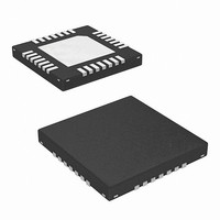
Pinout 2 ISL88550A ISL88550A (28 LD TQFN) TOP VIEW TON 1 OVP/UVP 2 REF 3 4 ILIM POK1 5 6 POK2 7 STBY LGATE 21 20 BOOT ...
Page 3
... DD Junction Temperature Range .-55°C to +150°C + 0.3V DD Operating Temperature Range . . . . . . . . . . . . . . . . .-40°C to +85°C + 0.3V DD Storage Temperature . . . . . . . . . . . . . . . . . . . . . . . . . -65°C + 150°C Pb-free reflow profile . . . . . . . . . . . . . . . . . . . . . . . . . .see link below http://www.intersil.com/pbfree/Pb-FreeReflow.asp + 0. SHDNA# = STBY# = BOOT = ILIM = 5V, OUT = REFIN = VTTI = 2.5V CONDITIONS FB = OUT FB = GND Rising edge of SHDNA# to full current limit ...
Page 4
Electrical Specifications V = +15V SKIP# = OVP/UVP = GND. PGND1 = PGND2 = PHASE = GND, VTTS = VTT, t +85°C, Unless otherwise specified, parts are 100% tested at +25°C. Temperature limits established by characterization ...
Page 5
Electrical Specifications V = +15V SKIP# = OVP/UVP = GND. PGND1 = PGND2 = PHASE = GND, VTTS = VTT, t +85°C, Unless otherwise specified, parts are 100% tested at +25°C. Temperature limits established by characterization ...
Page 6
Pin Descriptions PIN NAME 1 TON GND, REF OVP/UVP Overvoltage/Undervoltage Protection Control Input. This four-level logic input enables or disables the Overvoltage and/or Undervoltage Protection. The overvoltage ...
Page 7
Pin Descriptions (Continued) PIN NAME 19 PHASE External Inductor Connection. Connect PHASE to the input side of the inductor. PHASE is used for both current limit and the return supply of the UGATE driver. 20 BOOT Boost Flying-Capacitor Connection. Connect ...
Page 8
Typical Operating Characteristics 700 675 650 625 600 I = 12A OUT 575 550 525 500 475 450 OUT 425 400 (V) IN FIGURE 3. SWITCHING FREQUENCY vs INPUT ...
Page 9
Typical Operating Characteristics 0.95 0.94 0.93 0.92 0.91 0.90 0.89 0.88 0.87 0.86 0.85 -0.04 -0.03 -0.02 -0.01 0 LOAD (A) FIGURE 9. VTTR REGULATION vs VTTR LOAD I = 12A 15mA VDDQ VTTR 20µs/DIV FIGURE 11. LOAD ...
Page 10
Typical Operating Characteristics R = 10Ω 20Ω VDDQ VTT 2ms/DIV FIGURE 15. VDDQ START-UP AND SHUTDOWN INTO LIGHT LOAD, DISCHARGE ENABLED 50µs/DIV FIGURE 17. OVERVOLTAGE AND TURN-OFF OF BUCK OUTPUT UVP ENABLE 50µs/DIV FIGURE 19. SHORT CIRCUIT AND ...
Page 11
TON INTREF QUAD LEVEL OVP/UVP DECODER BUCK ON/OFF BLANK SHDNA# BIAS SHUTDOWN ON/OFF DECODER STBY# 0.7 x INTREF VTT ON/OFF VTTR ON/OFF INTREF+10% INTEREF-10% POK1 N FB INTREF/2 + 10% POK2 N INTEREF/2 - 10% 11 ISL88550A VIN t OFF ...
Page 12
Detailed Description The ISL88550A combines a synchronous buck PWM controller, an LDO linear regulator, and a 10mA reference output. The buck controller drives two external N-Channel MOSFETs to deliver load currents up to 15A and generates voltages down to 0.7V ...
Page 13
Specifications” table on page 3 are influenced by resistive losses and by switching delays in the high-side MOSFET. Resistive losses, which include the inductor, both MOSFETs, the output capacitors ESR, and any PC board copper losses in the output ...
Page 14
K-FACTOR TYPICAL K ERROR t SETTING FACTOR (µs) (10%) ON 200kHz 5.0 ± 300kHz 3.3 ± OPEN) ON 450kHz 2.2 ±12 REF) ON 600kHz 1.7 ±12 GND) ON ...
Page 15
1. LOAD(MAX) FIGURE 24. VALLEY CURRENT-LIMIT THRESHOLD POR, UVLO and Soft-Start Internal Power-on reset (POR) occurs when AV above approximately 2V, resetting the fault latch and the soft-start counter, powering up the ...
Page 16
ISL88550A pulls POK1 low. Any fault condition forces POK1 low until the fault latch is cleared by toggling SHDNA# or cycling AV 1V. For logic level output voltages, connect an external pull-up resistor between POK1 and ...
Page 17
OVP/UVP DISCHARGE AV 15Ω internal switch ON DD UGATE/LGATE is low when SHDNA# = low for normal shutdown OPEN 15Ω internal switch ON UGATE/LGATE is low when SHDNA# = low for normal shutdown REF 15Ω internal switch OFF UGATE/LGATE is ...
Page 18
ISL88550A TO ERROR AMPLIFIER FB + 0.1 x REF - (0.2V) FIGURE 25. DUAL-MODE FEEDBACK DECODER Setting the Buck Regulator Output (V Resistive Voltage-Divider at FB The Buck Regulator output voltage can be adjusted from 0.7V to 3.5V using a ...
Page 19
Most inductor manufacturers provide inductors in standard values, such as 1.0µH, 1.5µH, 2.2µH, 3.3µH, etc. Also look for nonstandard values, which can provide a better compromise in LIR across the input voltage range. If using a swinging inductor (where the ...
Page 20
MOSFET turning on, as this would result in shoot through current degrading the efficiency. MOSFETs with a lower ratio have higher immunity to dV/dt For proper ...
Page 21
Setting the Current Limit (Buck) The current-sense method used in the ISL88550A makes use of the ON-resistance ( the low side MOSFET DS(ON "Typical Application Circuit" on page 22). When 2 calculating the current limit, use ...
Page 22
Transient Response (Buck) The inductor ripple current also affects transient response performance, especially at low inductor values allow the inductor current to slew faster, replenishing charge removed from the output filter capacitors by a sudden load ...
Page 23
C3 1µF C9: OPEN AVDD AVDD R2 R3 100k Ω 100k Ω 1.8V C2 10µF PCI-e 1.2V/2A R9 1.21k Ω C4 2µFx10µF R10 4.99k Ω Applications Information Dropout Performance (Buck) The output voltage adjustable range for continuous conduction operation is ...
Page 24
... Accordingly, the reader is cautioned to verify that data sheets are current before placing orders. Information furnished by Intersil is believed to be accurate and reliable. However, no responsibility is assumed by Intersil or its subsidiaries for its use; nor for any infringements of patents or other rights of third parties which may result from its use ...
Page 25
Package Outline Drawing L28.5x5B 28 LEAD THIN QUAD FLAT NO-LEAD PLASTIC PACKAGE Rev 1, 10/07 5.00 6 PIN 1 INDEX AREA (4X) 0.15 TOP VIEW ( 4. 65 TYP ) ( 3. 25) TYPICAL RECOMMENDED LAND PATTERN 25 ISL88550A A ...