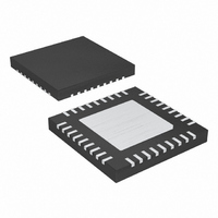
MAX1702BETX+ Maxim Integrated Products, MAX1702BETX+ Datasheet - Page 2

MAX1702BETX+
Manufacturer Part Number
MAX1702BETX+
Description
IC PWR MNG TRPL OUT 36-TQFN
Manufacturer
Maxim Integrated Products
Datasheet
1.MAX1702BETX.pdf
(19 pages)
Specifications of MAX1702BETX+
Applications
Processor
Voltage - Supply
2.6 V ~ 5.5 V
Operating Temperature
-40°C ~ 85°C
Mounting Type
Surface Mount
Package / Case
36-TQFN Exposed Pad
Lead Free Status / RoHS Status
Lead free / RoHS Compliant
Current - Supply
-
Lead Free Status / Rohs Status
Lead free / RoHS Compliant
ABSOLUTE MAXIMUM RATINGS
IN, FB2, OUT3, COMP1, COMP2, COMP3, PGM3,
REF to GND ...................................................-0.3 to (V
INP1, INP2, INP3 to IN...........................................-0.3V to +0.3V
PG1, PG2, PG3 to GND.........................................-0.3V to +0.3V
LX1, LX2, LX3 Continuous Current .......................-1.5A to +1.5A
INP1 to PG1..............................................................-0.3V to +6V
INP2 to PG2..............................................................-0.3V to +6V
Triple-Output Power-Management IC for
Microprocessor-Based Systems
Stresses beyond those listed under “Absolute Maximum Ratings” may cause permanent damage to the device. These are stress ratings only, and functional
operation of the device at these or any other conditions beyond those indicated in the operational sections of the specifications is not implied. Exposure to
absolute maximum rating conditions for extended periods may affect device reliability.
ELECTRICAL CHARACTERISTICS
(V
+85°C unless otherwise noted. Typical values are at T
2
INP1, INP2, INP3,
IN Supply Voltage Range
Undervoltage
Lockout Threshold
Quiescent Current
(I
SYNCHRONOUS BUCK PWM REGULATOR 1 (REG1)
OUT1 Voltage Accuracy
OUT1 Input Resistance
Error-Amp Transconductance
Dropout Voltage
P-Channel On-Resistance
N-Channel On-Resistance
Current-Sense Transresistance
P-Channel
Current-Limit Threshold
P-Channel Pulse-Skipping
Current Threshold
N-Channel Zero-Crossing
Comparator
OUT1 Maximum
Output Current
LX1 Leakage Current
LX1 Duty-Cycle Range
INP1
ON2, LBO, OUTOK, RSO, MR, LBI, DBI,
OUT1 to GND .......................................................-0.3V to +6V
INP1
_______________________________________________________________________________________
= V
+ I
INP2
INP2
PARAMETER
+ I
= V
INP3
INP3
+ I
= V
IN
)
IN
= 3.6V, V
INP1, INP2, INP3, IN must be connected together
externally
V
V
ON2 = IN, no load
ON2 = GND, no load
V
LX1-3 = GND
3.6V ≤ V
Load = 800mA (Note 1)
I
I
I
2.6V ≤ V
V
V
LX1
LX1
LX1
IN
IN
DBI
INP1
INP2
LBI
rising
falling
= 180mA
= 180mA, V
= 180mA
< 1.2 V (shutdown)
= 4.2V
= 5.5V, LX1= GND or INP1, V
= 1.1V, V
INP1
INP1
≤ 5.5V, load = 0 to 900mA
≤ 5.5V (Note 2)
IN
DBI
INP1
A
+ 0.3V)
= +25°C.)
CONDITIONS
= 1.35V, MR = ON2 = IN, PGM3 = GND, circuit of Figure 1, T
= 2.6V
INP3 to PG3..............................................................-0.3V to +6V
Output Short-Circuit Duration ............................................Infinite
Continuous Power Dissipation (T
Operating Temperature Range.............................40°C to +85°C
Junction Temperature ......................................................+150°C
Storage Temperature Range .............................-65°C to +150°C
Lead Temperature (soldering, 10sec) .............................+300°C
36-Pin QFN (derate 22.7 mW/°C)..............................1818mW
OUT1
= 3.6V
3.234
0.115
2.25
0.40
1.15
MIN
200
2.6
2.2
0.9
-20
55
25
0
A
1.275
0.140
=+70°C)
TYP
2.40
0.25
0.47
2.35
485
335
400
250
3.3
0.3
0.2
0.1
95
55
5
2.525
3.366
MAX
0.160
2.55
0.35
0.54
1.45
135
425
+20
100
5.5
0.4
0.5
20
75
A
= -40°C to
UNITS
V/A
mA
mV
µA
kΩ
µA
µS
%
Ω
Ω
V
V
V
A
A
A


