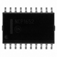
NCP1652DWR2G ON Semiconductor, NCP1652DWR2G Datasheet - Page 25

NCP1652DWR2G
Manufacturer Part Number
NCP1652DWR2G
Description
IC PFC CONTROLLER CCM/DCM 20SOIC
Manufacturer
ON Semiconductor
Datasheet
1.NCP1652DR2G.pdf
(34 pages)
Specifications of NCP1652DWR2G
Mode
Continuous Conduction (CCM), Discontinuous Conduction (DCM)
Frequency - Switching
100kHz
Current - Startup
5.62mA
Voltage - Supply
9.3 V ~ 20 V
Operating Temperature
-40°C ~ 125°C
Mounting Type
Surface Mount
Package / Case
20-SOIC (7.5mm Width)
Switching Frequency
20 KHz to 250 KHz
Maximum Operating Temperature
+ 125 C
Mounting Style
SMD/SMT
Minimum Operating Temperature
- 40 C
Lead Free Status / RoHS Status
Lead free / RoHS Compliant
Other names
NCP1652DWR2GOSTR
between the current sense resistor and the IS
to the low impedance of this amplifier. Any series resistance
due to a filter creates a voltage offset (V
bias current, CA
60 mA. The voltage offset is given by Equation 2.
The ac error amplifier will then try to compensate for the
average output current which appears never to go to zero and
cause additional zero crossing distortion.
applied to the IS
into a current, i
currents are generated, I
signal which is a replica of the instantaneous switch current.
I
V
AVG
ISPOS
Caution should be exercised when designing a filter
The offset adds a positive offset to the current sense signal.
A voltage proportional to the main switch current is
is a low frequency signal. The relationship between
and I
CS
POS
and I
V
1
Ibias
, and internally mirrored. Two internal
I
OS
p
pin. The IS
AVG
. The input bias current is typically
+ CA
R
R
IAVG
CS
CS
I
I
spos
AVG
is given by Equation 3.
and I
Ibias
POS
AVG
@ R
pin voltage is converted
external
. I
CS
Current sense
OS
is a high frequency
+
−
amplifier
) due to its input
g
Figure 63. Current Sense Amplifier
m
g
POS
m
= 250mS
input, due
(eq. 2)
http://onsemi.com
V
IAVG
25
blanking
blanking
t
t
LEB
LEB
the PWM input where it is added to the AC EA and ramp
compensation signal.
amplifier. This voltage signal is the product of I
external R
pin, C
significantly below the switching frequency to remove the
high frequency content. But, high enough to not to cause
significant distortion to the input full wave rectified
sinewave waveform. A properly filtered average current
signal has twice the line frequency. Equation 4 shows the
relationship between C
To AC error
amplifier
The PWM Output delivers current to the positive input of
The I
IAVG
AVG
Inst. current A
Inst. current B
IAVG
. The pole frequency, f
Output generates a voltage signal to a buffer
resistor filtered by the capacitor on the I
C
IAVG
I
CS
+
IAVG
+ I
2 @ p @ R
IN
(in nF) and f
To PWM
comparator
To PWM skip
comparator
+
V
1
P
ISPOS
, set by C
IAVG
4k
@ f
P
P
(in kHz).
IAVG
AVG
should be
(eq. 3)
(eq. 4)
and an
AVG


