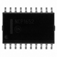
NCP1652DWR2G ON Semiconductor, NCP1652DWR2G Datasheet - Page 24

NCP1652DWR2G
Manufacturer Part Number
NCP1652DWR2G
Description
IC PFC CONTROLLER CCM/DCM 20SOIC
Manufacturer
ON Semiconductor
Datasheet
1.NCP1652DR2G.pdf
(34 pages)
Specifications of NCP1652DWR2G
Mode
Continuous Conduction (CCM), Discontinuous Conduction (DCM)
Frequency - Switching
100kHz
Current - Startup
5.62mA
Voltage - Supply
9.3 V ~ 20 V
Operating Temperature
-40°C ~ 125°C
Mounting Type
Surface Mount
Package / Case
20-SOIC (7.5mm Width)
Switching Frequency
20 KHz to 250 KHz
Maximum Operating Temperature
+ 125 C
Mounting Style
SMD/SMT
Minimum Operating Temperature
- 40 C
Lead Free Status / RoHS Status
Lead free / RoHS Compliant
Other names
NCP1652DWR2GOSTR
ISpos pin multiplied by the current sense amplifier gain. It
is applied to the inverting input of the AC EA.
transconductance amplifier generates an output current
proportional to its differential input voltage. This amplifier
has a nominal gain of 100 mS (or 0.0001 A/V). That is, an
input voltage difference of 10 mV causes the output current
to change by 1.0 mA. The AC EA has typical source and sink
currents of 70 mA.
frequency pole forces the average input current to follow the
by I
ramp compensation current. OUTA is terminated once the
voltage at the PWM non-inverting input reaches 4 V.
Current Sense Amplifier
applied to the current sense input, IS
The AC EA is a transconductance amplifier. A
The filtered input current is a high frequency signal. A low
The voltage at the PWN non-inverting input is determined
A voltage proportional to the main switch current is
ACEA(out)
R
IAVG
, the instantaneous switch current along and the
I
ACEA(out)
I
AVG
+
2.8 * V
V
AC_REF
37.33k
POS
ACEA
. The current sense
+
−
gm
amplifier
AC COMP
g
AC error
Figure 62. AC EA Buffer Amplifier
@ 4
m
= 100mS
2.8V
+
(eq. 1)
http://onsemi.com
R
AC_COMP
24
+
+
−
−
reference generator output. A pole-zero pair is created by
placing a (R
combination at the output of the AC EA. The AC COMP pin
provides access to the AC EA output.
current using a second transconductance amplifier. The
output of the inverting transconductance amplifier is
V
AC EA buffer. The AC EA buffer output current, I
is given by Equation 1.
amplifier is a wide bandwidth amplifier with a differential
input. The current sense amplifier has two outputs, PWM
Output and I
instantaneous switch current which is filtered by the internal
leading edge blanking (LEB) circuitry prior to applying it to
the PWM Comparator non inverting input. The second
output is a filtered current signal resembling the average
value of the input current. Figure 63 shows the internal
architecture of the current sense amplifier.
ACEA(buffer).
The output of the AC EA is inverted and converted into a
VDD
Figure 62 shows the circuit schematic of the
AVG
COMP
37.33kW
x 4
Output. The PWM Output is the
) and capacitor (C
I
ACEA(out)
21.33kW
comparator
To PWM
COMP
ACEA(out)
) series
,


