AMIS30542C5421RG ON Semiconductor, AMIS30542C5421RG Datasheet - Page 24
AMIS30542C5421RG
Manufacturer Part Number
AMIS30542C5421RG
Description
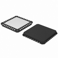
IC MOTOR DVR MICRO STEP 32QFP
Manufacturer
ON Semiconductor
Type
Micro Stepping Motor Driverr
Datasheet
1.AMIS30542C5421RG.pdf
(29 pages)
Specifications of AMIS30542C5421RG
Applications
Stepper Motor Driver, 2 Phase
Number Of Outputs
1
Current - Output
2.2A
Voltage - Supply
6 V ~ 30 V
Operating Temperature
-40°C ~ 125°C
Mounting Type
Surface Mount
Package / Case
32-VSQFP
Product
Stepper Motor Controllers / Drivers
Operating Supply Voltage
6 V to 30 V
Supply Current
8 mA
Mounting Style
SMD/SMT
Lead Free Status / RoHS Status
Lead free / RoHS Compliant
Voltage - Load
-
Lead Free Status / Rohs Status
Lead free / RoHS Compliant
Available stocks
Company
Part Number
Manufacturer
Quantity
Price
Company:

Part Number:
AMIS30542C5421RG
Manufacturer:
ON Semiconductor
Quantity:
1 500
Company:
Part Number:
AMIS30542C5421RG
Manufacturer:
ON Semiconductor
Quantity:
10 000


NOTE:
Where:
R/W
Reset:
Table 13. SPI CONTROL REGISTERS
hard reset)
Figure 23. A WRITE Operation Where DATA from the Master is Written in SPI Register with Address 2 Followed
CR0 (01h)
CR1 (02h)
CR2 (03h)
CR2 (08h)
WR (00h)
Address
The internal data−out shift buffer of AMIS−30542 is updated with the content of the selected SPI register only at the last (every
eight) falling edge of the CLK signal (see SPI Transfer Format and Pin Signals). As a result, new data for transmission cannot be
written to the shift buffer at the beginning of the transfer packet and the first byte shifted out might represent old data.
DO
CS
DI
DATA from previous
command or NOT VALID
after POR or RESET
Read and Write access
Status after power−On or hard reset
Content
Access
Reset
Data
Data
Data
Data
Data
by a READ Back Operation to Confirm a Correct WRITE Operation
Registers are updated with
the internal status at the
rising edge of CS
COMMAND
WRITE DATA
or NOT VALID
DIRCTRL
OLD DATA
MOTEN
to ADDR2
WDEN
DATA
Bit 7
R/W
0
M[1:0]
(All SPI control registers have Read/Write Access and default to “0” after power−on or
SM[2:0]
NXTP
Bit 6
R/W
SLP
0
http://onsemi.com
from ADDR2
NEW DATA
DATA
OLD DATA
for ADDR2
DATA
SLAG
Bit 5
R/W
0
−
24
WDT[3:0]
StrB[1:0]
SLAT
Bit 4
R/W
COMMAND
0
−
READ DATA
from ADDR2
from ADDR2
OLD DATA
Structure
DATA
The NEW DATA is written into the
corresponding internal register at
the rising edge of CS
PWMF
Bit 3
R/W
0
−
−
CUR[4:0]
from ADDR2
COMMAND
NEW DATA
or DUMMY
PWMJ
DATA
Bit 2
R/W
StrC
0
−
−
Bit 1
R/W
0
−
−
EMC[1:0]
StrE[1:0]
Bit 0
R/W
0
−
−
Related parts for AMIS30542C5421RG
Image
Part Number
Description
Manufacturer
Datasheet
Request
R

Part Number:
Description:
ON Semiconductor [VOLTAGE REGULATOR]
Manufacturer:
ON Semiconductor
Datasheet:
Part Number:
Description:
357-036-542-201 CARDEDGE 36POS DL .156 BLK LOPRO
Manufacturer:
ON Semiconductor
Datasheet:
Part Number:
Description:
357-036-542-201 CARDEDGE 36POS DL .156 BLK LOPRO
Manufacturer:
ON Semiconductor
Datasheet:
Part Number:
Description:
357-036-542-201 CARDEDGE 36POS DL .156 BLK LOPRO
Manufacturer:
ON Semiconductor
Datasheet:
Part Number:
Description:
357-036-542-201 CARDEDGE 36POS DL .156 BLK LOPRO
Manufacturer:
ON Semiconductor
Datasheet:
Part Number:
Description:
357-036-542-201 CARDEDGE 36POS DL .156 BLK LOPRO
Manufacturer:
ON Semiconductor
Datasheet:
Part Number:
Description:
357-036-542-201 CARDEDGE 36POS DL .156 BLK LOPRO
Manufacturer:
ON Semiconductor
Datasheet:
Part Number:
Description:
357-036-542-201 CARDEDGE 36POS DL .156 BLK LOPRO
Manufacturer:
ON Semiconductor
Datasheet:
Part Number:
Description:
357-036-542-201 CARDEDGE 36POS DL .156 BLK LOPRO
Manufacturer:
ON Semiconductor
Datasheet:
Part Number:
Description:
357-036-542-201 CARDEDGE 36POS DL .156 BLK LOPRO
Manufacturer:
ON Semiconductor
Datasheet:
Part Number:
Description:
357-036-542-201 CARDEDGE 36POS DL .156 BLK LOPRO
Manufacturer:
ON Semiconductor
Datasheet:
Part Number:
Description:
Manufacturer:
ON Semiconductor
Datasheet:
Part Number:
Description:
Manufacturer:
ON Semiconductor
Datasheet:
Part Number:
Description:
Manufacturer:
ON Semiconductor
Datasheet: