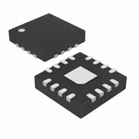
MAX6946ATE+ Maxim Integrated Products, MAX6946ATE+ Datasheet - Page 8

MAX6946ATE+
Manufacturer Part Number
MAX6946ATE+
Description
IC LED DRIVER LINEAR 16-TQFN
Manufacturer
Maxim Integrated Products
Type
Linear (I²C Interface)r
Datasheet
1.MAX6947ATE.pdf
(24 pages)
Specifications of MAX6946ATE+
Constant Current
Yes
Topology
Open Drain, PWM
Number Of Outputs
10
Internal Driver
Yes
Type - Primary
Backlight
Type - Secondary
RGB, White LED
Frequency
400kHz
Voltage - Supply
2.25 V ~ 3.6 V
Voltage - Output
7V
Mounting Type
Surface Mount
Package / Case
16-TQFN Exposed Pad
Operating Temperature
-40°C ~ 125°C
Current - Output / Channel
20mA
Internal Switch(s)
Yes
Number Of Segments
3
Low Level Output Current
21120 uA
Operating Supply Voltage
2.25 V to 3.6 V
Maximum Supply Current
4 mA
Maximum Power Dissipation
1176 mW
Maximum Operating Temperature
+ 125 C
Mounting Style
SMD/SMT
Minimum Operating Temperature
- 40 C
Lead Free Status / RoHS Status
Lead free / RoHS Compliant
Efficiency
-
Lead Free Status / Rohs Status
Lead free / RoHS Compliant
Use the configuration register to select PWM phasing
between outputs, test fade status, enable hardware
startup from shutdown, and select shutdown or run
mode (Table 2).
Table 2. Configuration Register (0x10)
Table 3. Initial Power-Up Register Status
10-Port, Constant-Current LED Driver and
I/O Expander with PWM Intensity Control
*The OSCEN bit applies only to the MAX6946. OSCEN is always 0 for the MAX6947, and the MAX6947 ignores writes to the OSCEN bit.
**Read-only bits.
*Value is 0 for MAX6947 and 1 for MAX6946 bit.
8
Port P0–P9 output level
or PWM
Configuration
Ramp-down/hold-off
Ramp-up
Output current ISET70
Output current ISET98
Global current
REGISTER BIT
_______________________________________________________________________________________
DESCRIPTION
D7
D6
D5
D4
D3
D2
D1
D0
Configuration Register (0x10)
OSC enable*
RSTPOR options
PWM stagger
Hold-off status**
Fade-off status**
Ramp-up status**
RST RUN enable
RUN enable
DESCRIPTION
Port 0–9 high impedance
S hutd ow n m od e, Reset Run d i sab l ed
Fade/hold-off disabled
Disabled
I
I
Full current
PEAK
PEAK
POWER-UP CONDITION
= 10mA for ports P7–P0
= 10mA for ports P9, P8
VALUE
0
1
0
1
0
1
0
1
0
1
0
1
0
1
0
1
Internal oscillator enabled as PWM clock source
External oscillator input enabled as PWM clock source
RST does not change register data
RST resets registers to POR (power-on reset) state
PWM outputs are in phase
PWM outputs stagger phase
Device not in hold-off
Device in hold-off
Device not in fade-off
Device in fade-off
Device not in ramp-up
Device in ramp-up
Reset Run disabled
Reset Run enabled
Shutdown mode
Run mode
CODE (HEX)
ADDRESS
0x00–0x09
All control registers reset upon power-up (Table 3).
Power-up status sets I/O ports P0 to P9 to high imped-
ance, and puts the device into shutdown. The
MAX6946/MAX6947 powers up in shutdown.
0x10
0x11
0x12
0x13
0x14
0x15
0/1*
D7
1
0
0
0
0
0
D6
1
0
0
0
0
0
0
FUNCTION
D5
1
0
0
0
0
0
0
REGISTER BIT
D4
1
0
0
0
0
0
0
D3
Initial Power-Up
1
0
0
0
0
0
0
D2
1
0
0
0
0
0
1
D1
1
0
0
0
0
0
1
D0
1
0
0
0
0
0
1


