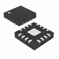
MAX6946ATE+ Maxim Integrated Products, MAX6946ATE+ Datasheet - Page 6

MAX6946ATE+
Manufacturer Part Number
MAX6946ATE+
Description
IC LED DRIVER LINEAR 16-TQFN
Manufacturer
Maxim Integrated Products
Type
Linear (I²C Interface)r
Datasheet
1.MAX6947ATE.pdf
(24 pages)
Specifications of MAX6946ATE+
Constant Current
Yes
Topology
Open Drain, PWM
Number Of Outputs
10
Internal Driver
Yes
Type - Primary
Backlight
Type - Secondary
RGB, White LED
Frequency
400kHz
Voltage - Supply
2.25 V ~ 3.6 V
Voltage - Output
7V
Mounting Type
Surface Mount
Package / Case
16-TQFN Exposed Pad
Operating Temperature
-40°C ~ 125°C
Current - Output / Channel
20mA
Internal Switch(s)
Yes
Number Of Segments
3
Low Level Output Current
21120 uA
Operating Supply Voltage
2.25 V to 3.6 V
Maximum Supply Current
4 mA
Maximum Power Dissipation
1176 mW
Maximum Operating Temperature
+ 125 C
Mounting Style
SMD/SMT
Minimum Operating Temperature
- 40 C
Lead Free Status / RoHS Status
Lead free / RoHS Compliant
Efficiency
-
Lead Free Status / Rohs Status
Lead free / RoHS Compliant
10-Port, Constant-Current LED Driver and
I/O Expander with PWM Intensity Control
6
MAX6946/
MAX6947
_______________________________________________________________________________________
10
11
12
13
14
15
16
—
1
2
3
4
5
6
7
8
9
**MAX6946 ONLY.
**MAX6947 ONLY.
PIN
MAX6946C
ADO**
SDA
SCL
RST
B4
B3
C4
C3
D4
D3
D2
D1
C2
C1
B1
B2
A1
A2
A3
A4
OSC*
—
MAX6946
MAX6947
EXTERNAL CLOCK INPUT*
CURRENT REFERENCE
OSC (MAX6946)
AD0 (MAX6947)
OSCILLATOR
INTERNAL
NAME
GND
VDD
SDA
RST
SCL
P0
P1
P2
P3
P4
P5
P6
P7
P8
P9
EP
CONFIGURATION
REGISTER
I/O Ports. Configure P0–P4 as open-drain current sink outputs rated at
20mA (max), as CMOS-logic inputs, or as open-drain logic outputs.
Connect loads to a supply voltage no higher than 7V.
Ground
I/O Ports. Configure P5–P9 as open-drain current sink outputs rated at
20mA (max), as CMOS-logic inputs, or as open-drain logic outputs.
Connect loads to a supply voltage no higher than 7V.
External Oscillator Input
Address Input. Sets the device slave address (see Table 10).
Active-Low Reset Input
P osi ti ve S up p l y V ol tag e. Byp ass V D D to GN D w i th a 0.1µF cer am i c cap aci tor .
I
I
Exposed Pad on Package Underside. Connect to GND. Do not use as the
main ground connection.
2
2
C-Compatible, Serial-Clock Input
C-Compatible, Serial-Data I/O
2-WIRE SERIAL INTERFACE
RAMP-UP/RAMP-DOWN
PWM CONTROLLER
CONTROLS
I/O REGISTER
I/O PORTS
FUNCTION
Pin Description
Block Diagram
P0
P1
P2
P3
P4
P5
P6
P7
P8
P9


