PCA9632DP1,118 NXP Semiconductors, PCA9632DP1,118 Datasheet - Page 5
PCA9632DP1,118
Manufacturer Part Number
PCA9632DP1,118
Description
IC LED DRIVER RGBA 8-TSSOP
Manufacturer
NXP Semiconductors
Type
RGBA LED Driverr
Datasheet
1.PCA9632TK118.pdf
(38 pages)
Specifications of PCA9632DP1,118
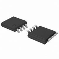
Package / Case
8-TSSOP
Topology
Open Drain, PWM
Number Of Outputs
4
Internal Driver
Yes
Type - Primary
Backlight, LED Blinker
Type - Secondary
RGBA
Frequency
1MHz
Voltage - Supply
2.3 V ~ 5.5 V
Voltage - Output
5.5V
Mounting Type
Surface Mount
Operating Temperature
-40°C ~ 85°C
Current - Output / Channel
25mA
Internal Switch(s)
Yes
Number Of Segments
4
Low Level Output Current
100000 uA
Operating Supply Voltage
2.3 V to 5.5 V
Maximum Supply Current
150 uA
Maximum Power Dissipation
400 mW
Maximum Operating Temperature
+ 85 C
Mounting Style
SMD/SMT
Minimum Operating Temperature
- 40 C
Lead Free Status / RoHS Status
Lead free / RoHS Compliant
Efficiency
-
Lead Free Status / Rohs Status
Lead free / RoHS Compliant
Other names
935284899118
PCA9632DP1-T
PCA9632DP1-T
PCA9632DP1-T
PCA9632DP1-T
Available stocks
Company
Part Number
Manufacturer
Quantity
Price

Part Number:
PCA9632DP1,118
Manufacturer:
NXP/恩智浦
Quantity:
20 000


NXP Semiconductors
6. Pinning information
PCA9632_3
Product data sheet
6.1 Pinning
6.2 Pin description
Table 2.
[1]
Symbol
LED0
LED1
LED2
LED3
V
SCL
SDA
V
Fig 2.
Fig 4.
SS
DD
HVSON8 package die supply ground is connected to both the V
V
and board-level performance, the exposed pad needs to be soldered to the board using a corresponding
thermal pad on the board, and for proper heat conduction through the board thermal vias need to be
incorporated in the PCB in the thermal pad region.
index area
terminal 1
SS
pin must be connected to supply ground for proper device operation. For enhanced thermal, electrical,
LED0
LED1
LED2
LED3
LED0
LED1
LED2
LED3
Pin configuration for TSSOP8
Pin configuration for HVSON8
Pin description for TSSOP8 and HVSON8
Pin
1
2
3
4
5
6
7
8
[1]
1
2
3
4
1
2
3
4
PCA9632DP1
Transparent top view
Type
O
O
O
O
power supply
I
I/O
power supply
PCA9632TK
002aad040
Rev. 03 — 15 July 2008
002aad041
8
7
6
5
V
SDA
SCL
V
8
7
6
5
Description
LED driver 0
LED driver 1
LED driver 2
LED driver 3
supply ground
serial clock line
serial data line
supply voltage
DD
SS
V
SDA
SCL
V
DD
SS
Fig 3.
Fig 5.
4-bit Fm+ I
index area
terminal 1
LED0
LED1
LED2
LED3
LED0
LED1
LED2
LED3
A0
Pin configuration for TSSOP10
Pin configuration for HVSON10
SS
A0
pin and the exposed center pad. The
1
2
3
4
5
2
C-bus low power LED driver
1
2
3
4
5
PCA9632DP2
Transparent top view
PCA9632TK2
002aad637
PCA9632
© NXP B.V. 2008. All rights reserved.
002aad638
10
9
8
7
6
10
V
SDA
SCL
A1
V
9
8
7
6
DD
SS
V
SDA
SCL
A1
V
DD
SS
5 of 38
Related parts for PCA9632DP1,118
Image
Part Number
Description
Manufacturer
Datasheet
Request
R

Part Number:
Description:
NXP Semiconductors designed the LPC2420/2460 microcontroller around a 16-bit/32-bitARM7TDMI-S CPU core with real-time debug interfaces that include both JTAG andembedded trace
Manufacturer:
NXP Semiconductors
Datasheet:

Part Number:
Description:
NXP Semiconductors designed the LPC2458 microcontroller around a 16-bit/32-bitARM7TDMI-S CPU core with real-time debug interfaces that include both JTAG andembedded trace
Manufacturer:
NXP Semiconductors
Datasheet:
Part Number:
Description:
NXP Semiconductors designed the LPC2468 microcontroller around a 16-bit/32-bitARM7TDMI-S CPU core with real-time debug interfaces that include both JTAG andembedded trace
Manufacturer:
NXP Semiconductors
Datasheet:
Part Number:
Description:
NXP Semiconductors designed the LPC2470 microcontroller, powered by theARM7TDMI-S core, to be a highly integrated microcontroller for a wide range ofapplications that require advanced communications and high quality graphic displays
Manufacturer:
NXP Semiconductors
Datasheet:
Part Number:
Description:
NXP Semiconductors designed the LPC2478 microcontroller, powered by theARM7TDMI-S core, to be a highly integrated microcontroller for a wide range ofapplications that require advanced communications and high quality graphic displays
Manufacturer:
NXP Semiconductors
Datasheet:
Part Number:
Description:
The Philips Semiconductors XA (eXtended Architecture) family of 16-bit single-chip microcontrollers is powerful enough to easily handle the requirements of high performance embedded applications, yet inexpensive enough to compete in the market for hi
Manufacturer:
NXP Semiconductors
Datasheet:
Part Number:
Description:
The XA-S3 device is a member of Philips Semiconductors? XA(eXtended Architecture) family of high performance 16-bitsingle-chip microcontrollers
Manufacturer:
NXP Semiconductors
Datasheet:

Part Number:
Description:
The NXP BlueStreak LH75401/LH75411 family consists of two low-cost 16/32-bit System-on-Chip (SoC) devices
Manufacturer:
NXP Semiconductors
Datasheet:
Part Number:
Description:
The NXP LPC3130/3131 combine an 180 MHz ARM926EJ-S CPU core, high-speed USB2
Manufacturer:
NXP Semiconductors
Datasheet:
Part Number:
Description:
The NXP LPC3141 combine a 270 MHz ARM926EJ-S CPU core, High-speed USB 2
Manufacturer:
NXP Semiconductors
Part Number:
Description:
The NXP LPC3143 combine a 270 MHz ARM926EJ-S CPU core, High-speed USB 2
Manufacturer:
NXP Semiconductors

Part Number:
Description:
The NXP LPC3152 combines an 180 MHz ARM926EJ-S CPU core, High-speed USB 2
Manufacturer:
NXP Semiconductors
Part Number:
Description:
The NXP LPC3154 combines an 180 MHz ARM926EJ-S CPU core, High-speed USB 2
Manufacturer:
NXP Semiconductors

Part Number:
Description:
Standard level N-channel enhancement mode Field-Effect Transistor (FET) in a plastic package using NXP High-Performance Automotive (HPA) TrenchMOS technology
Manufacturer:
NXP Semiconductors
Datasheet: