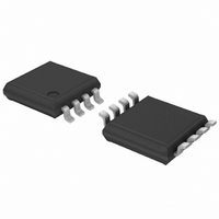
PCA9632DP1,118 NXP Semiconductors, PCA9632DP1,118 Datasheet - Page 14

PCA9632DP1,118
Manufacturer Part Number
PCA9632DP1,118
Description
IC LED DRIVER RGBA 8-TSSOP
Manufacturer
NXP Semiconductors
Type
RGBA LED Driverr
Datasheet
1.PCA9632TK118.pdf
(38 pages)
Specifications of PCA9632DP1,118
Package / Case
8-TSSOP
Topology
Open Drain, PWM
Number Of Outputs
4
Internal Driver
Yes
Type - Primary
Backlight, LED Blinker
Type - Secondary
RGBA
Frequency
1MHz
Voltage - Supply
2.3 V ~ 5.5 V
Voltage - Output
5.5V
Mounting Type
Surface Mount
Operating Temperature
-40°C ~ 85°C
Current - Output / Channel
25mA
Internal Switch(s)
Yes
Number Of Segments
4
Low Level Output Current
100000 uA
Operating Supply Voltage
2.3 V to 5.5 V
Maximum Supply Current
150 uA
Maximum Power Dissipation
400 mW
Maximum Operating Temperature
+ 85 C
Mounting Style
SMD/SMT
Minimum Operating Temperature
- 40 C
Lead Free Status / RoHS Status
Lead free / RoHS Compliant
Efficiency
-
Lead Free Status / Rohs Status
Lead free / RoHS Compliant
Other names
935284899118
PCA9632DP1-T
PCA9632DP1-T
PCA9632DP1-T
PCA9632DP1-T
Available stocks
Company
Part Number
Manufacturer
Quantity
Price
Part Number:
PCA9632DP1,118
Manufacturer:
NXP/恩智浦
Quantity:
20 000
NXP Semiconductors
PCA9632_3
Product data sheet
7.3.5 Group frequency, GRPFREQ
7.3.6 LED driver output state, LEDOUT
7.3.7 I
Table 10.
Legend: * default value.
GRPFREQ is used to program the global blinking period when DMBLNK bit (MODE2
register) is equal to logic 1. Value in this register is a ‘don’t care’ when DMBLNK = 0.
Applicable to LED outputs programmed with LDRx = 11 (LEDOUT register).
Blinking period is controlled through 256 linear steps from 00h (41 ms, frequency 24 Hz)
to FFh (10.73 seconds).
Table 11.
Legend: * default value.
LDRx = 00 — LED driver x is off (default power-up state).
LDRx = 01 — LED driver x is fully on (individual brightness and group dimming/blinking
not controlled).
LDRx = 10 — LED driver x individual brightness can be controlled through its PWMx
register.
LDRx = 11 — LED driver x individual brightness and group dimming/blinking can be
controlled through its PWMx register and the GRPPWM registers.
Table 12.
Legend: * default value.
Subaddresses are programmable through the I
E4h, E8h, and the device(s) will not acknowledge these addresses right after power-up
(the corresponding SUBx bit in MODE1 register is equal to logic 0).
global blinking period
Address
07h
Address
08h
Address
09h
0Ah
0Bh
2
C-bus subaddress 1 to 3, SUBADRx
Register
SUBADR1
SUBADR2
SUBADR3
GRPFREQ - Group frequency register (address 07h) bit description
Register
GRPFREQ
LEDOUT - LED driver output state register (address 08h) bit description
Register
LEDOUT
SUBADR1 to SUBADR3 - I
0Bh) bit description
Bit
7:0
Bit
7:6
5:4
3:2
1:0
Rev. 03 — 15 July 2008
Bit
7:1
0
7:1
0
7:1
0
=
GFRQ 7:0
--------------------------------------- - in
Symbol
GFRQ[7:0]
Symbol
LDR3
LDR2
LDR1
LDR0
Symbol
A1[7:1]
A1[0]
A2[7:1]
A2[0]
A3[7:1]
A3[0]
24
2
C-bus subaddress registers 0 to 3 (address 09h to
+
1
Access Value
R/W
Access Value
R/W
R/W
R/W
R/W
Access Value
R/W
R only
R/W
R only
R/W
R only
sec
2
4-bit Fm+ I
C-bus. Default power-up values are E2h,
onds
0000 0000* GRPFREQ register
00*
00*
00*
00*
1110 001*
0*
1110 010*
0*
1110 100*
0*
2
C-bus low power LED driver
Description
Description
LED3 output state control
LED2 output state control
LED1 output state control
LED0 output state control
Description
I
reserved
I
reserved
I
reserved
2
2
2
C-bus subaddress 1
C-bus subaddress 2
C-bus subaddress 3
PCA9632
© NXP B.V. 2008. All rights reserved.
14 of 38
(7)


