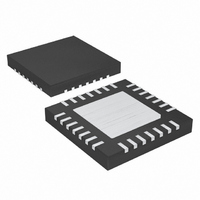
MAX16818ETI+ Maxim Integrated Products, MAX16818ETI+ Datasheet - Page 8

MAX16818ETI+
Manufacturer Part Number
MAX16818ETI+
Description
IC LED DRIVR PWM CONTROL 28-TQFN
Manufacturer
Maxim Integrated Products
Type
PWM Controlr
Datasheet
1.MAX16818ETI.pdf
(25 pages)
Specifications of MAX16818ETI+
Topology
High Side, Low Side, PWM, SEPIC, Step-Down (Buck), Step-Up (Boost)
Number Of Outputs
1
Internal Driver
No
Type - Primary
Automotive, Backlight
Type - Secondary
High Brightness LED (HBLED)
Frequency
125kHz ~ 1.5MHz
Voltage - Supply
4.75 V ~ 5.5 V, 7 V ~ 28 V
Voltage - Output
5.1V
Mounting Type
Surface Mount
Package / Case
28-TQFN Exposed Pad
Operating Temperature
-40°C ~ 85°C
Current - Output / Channel
30A
Internal Switch(s)
Yes
Low Level Output Current
4 A
High Level Output Current
4000000 uA (Typ)
Operating Supply Voltage
7 V to 28 V
Maximum Supply Current
5.5 mA
Maximum Power Dissipation
2758 mW
Maximum Operating Temperature
+ 85 C
Mounting Style
SMD/SMT
Minimum Operating Temperature
- 40 C
Lead Free Status / RoHS Status
Lead free / RoHS Compliant
Efficiency
-
Lead Free Status / Rohs Status
Lead free / RoHS Compliant
1.5MHz, 30A High-Efficiency, LED Driver
with Rapid LED Current Pulsing
8
_______________________________________________________________________________________
PIN
21
23
24
26
27
28
—
SENSE+
SENSE-
NAME
CSP
V
V
EP
IN
CC
DD
Current-Sense Differential Amplifier Positive Input. The differential voltage between CSN and CSP is
amplified internally by the current-sense amplifier (gain = 34.5) to measure the inductor current.
Differential LED Current-Sensing Negative Input. SENSE- is used to sense the LED current. Connect
SENSE- to the negative side of the LED current-sense resistor.
Differential LED Current-Sensing Positive Input. SENSE+ is used to sense the LED current. Connect
SENSE+ to the positive side of the LED current-sense resistor.
Supply Voltage Connection. Connect IN to V
Internal +5V Regulator Output. V
and 0.1µF ceramic capacitors.
Supply Voltage for Low-Side and High-Side Drivers. Connect a parallel combination of 0.1µF and 1µF
ceramic capacitors to PGND and a 1Ω resistor to V
from internal circuitry.
Exposed Paddle. Connect the exposed paddle to a copper pad (SGND) to improve power
dissipation.
CC
is derived from the IN voltage. Bypass V
CC
FUNCTION
for a +5V system.
CC
Pin Description (continued)
to filter out the high peak currents of the driver
CC
to SGND with 4.7µF


