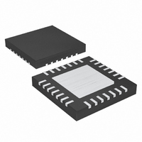
MAX16818ETI+ Maxim Integrated Products, MAX16818ETI+ Datasheet - Page 24

MAX16818ETI+
Manufacturer Part Number
MAX16818ETI+
Description
IC LED DRIVR PWM CONTROL 28-TQFN
Manufacturer
Maxim Integrated Products
Type
PWM Controlr
Datasheet
1.MAX16818ETI.pdf
(25 pages)
Specifications of MAX16818ETI+
Topology
High Side, Low Side, PWM, SEPIC, Step-Down (Buck), Step-Up (Boost)
Number Of Outputs
1
Internal Driver
No
Type - Primary
Automotive, Backlight
Type - Secondary
High Brightness LED (HBLED)
Frequency
125kHz ~ 1.5MHz
Voltage - Supply
4.75 V ~ 5.5 V, 7 V ~ 28 V
Voltage - Output
5.1V
Mounting Type
Surface Mount
Package / Case
28-TQFN Exposed Pad
Operating Temperature
-40°C ~ 85°C
Current - Output / Channel
30A
Internal Switch(s)
Yes
Low Level Output Current
4 A
High Level Output Current
4000000 uA (Typ)
Operating Supply Voltage
7 V to 28 V
Maximum Supply Current
5.5 mA
Maximum Power Dissipation
2758 mW
Maximum Operating Temperature
+ 85 C
Mounting Style
SMD/SMT
Minimum Operating Temperature
- 40 C
Lead Free Status / RoHS Status
Lead free / RoHS Compliant
Efficiency
-
Lead Free Status / Rohs Status
Lead free / RoHS Compliant
1.5MHz, 30A High-Efficiency, LED Driver
with Rapid LED Current Pulsing
Use the following guidelines to layout the switching volt-
age regulator:
1) Place the IN, V
2) Minimize the area and length of the high current
3) Keep short the current loop formed by the lower
4) Place the Schottky diodes close to the lower
5) Keep the SGND and PGND isolated and connect
6) Run the current-sense lines CSP and CSN very
7) Avoid long traces between the V
8) Distribute the power components evenly across the
9) Provide enough copper area at and around the
10) Use wide copper traces (2oz) to keep trace induc-
24
close to the MAX16818.
loops from the input capacitor, upper switching
MOSFET, inductor, and output capacitor back to
the input capacitor negative terminal.
switching MOSFET, inductor, and output capacitor.
MOSFETs and on the same side of the PCB.
them at one single point.
close to each other to minimize the loop area.
Similarly, run the remote voltage-sense lines
SENSE+ and SENSE- close to each other. Do not
cross these critical signal lines through power cir-
cuitry. Sense the current right at the pads of the
current-sense resistors.
tors, the driver output of the MAX16818, the MOS-
FET gates, and PGND. Minimize the loop formed by
the V
strap capacitor, the MAX16818, and the upper
MOSFET gate.
board for proper heat dissipation.
switching MOSFETs, inductor, and sense resistors
to aid in thermal dissipation.
tance and resistance low to maximize efficiency.
Wide traces also cool heat-generating components.
______________________________________________________________________________________
CC
bypass capacitors, bootstrap diode, boot-
CC
, and V
PCB Layout Guidelines
DD
bypass capacitors
DD
bypass capaci-
For the latest package outline information and land patterns, go
to www.maxim-ic.com/packages.
TRANSISTOR COUNT: 5654
PROCESS: BiCMOS
PACKAGE TYPE
28 TQFN
TOP VIEW
22
23
24
25
26
27
28
+
21
1
* EXPOSED PAD
PACKAGE CODE
20
2
Package Information
19
T2855-3
3
MAX16818
TQFN
18
Pin Configuration
4
Chip Information
17
5
16
6
15
7
DOCUMENT NO.
14
13
12
11
10
9
8
21-0140


