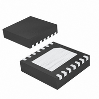
DS1842N+T&R Maxim Integrated Products, DS1842N+T&R Datasheet - Page 5

DS1842N+T&R
Manufacturer Part Number
DS1842N+T&R
Description
IC CURRENT MONITOR 14TDFN
Manufacturer
Maxim Integrated Products
Datasheet
1.DS1842NTR.pdf
(7 pages)
Specifications of DS1842N+T&R
Function
Current Monitor
Operating Temperature
-40°C ~ 85°C
Mounting Type
Surface Mount
Package / Case
14-TDFN Exposed Pad
Lead Free Status / RoHS Status
Lead free / RoHS Compliant
Current - Output
-
Voltage - Input
-
Accuracy
-
Sensing Method
-
Lead Free Status / Rohs Status
Lead free / RoHS Compliant
Figure 1. Current Clamp from Current Feedback
The DS1842 contains discrete high-voltage compo-
nents required to create an APD bias voltage and to
monitor the APD bias current. The device’s mirror out-
puts are a current that is a precise ratio of the output
current across a large dynamic range. The mirror
response time is fast enough to comply with GPON Rx
burst-mode monitoring requirements. The device has a
built-in current-limiting feature to protect APDs. The
APD current can also be shut down by CLAMP or ther-
mal shutdown. The internal FET is used in conjunction
with a DC-DC boost controller to precisely create the
APD bias voltage.
The DS1842 has two current mirror outputs. One is a
10:1 mirror connected at MIR1, and the other is a 5:1
mirror connected to MIR2.
The mirror output is typically connected to an ADC
using a resistor to convert the mirrored current into a
voltage. The resistor to ground should be selected such
that the maximum full-scale voltage of the ADC is
reached when the maximum mirrored current is
reached. For example, if the maximum monitored cur-
rent through the APD is 2mA with a 1V ADC full scale,
MIR1
REF
_______________________________________________________________________________________
Detailed Description
76V, APD, Bias Output Stage with
Current Mirror
CLAMP
and the 10:1 mirror is used, then the correct resistor is
approximately 5kΩ. If both MIR1 and MIR2 are con-
nected together, the correct resistor is 1.6kΩ.
The mirror response time is dominated by the amount
of capacitance placed on the output. For burst-mode
Rx systems where the fastest response times are
required (approximately a 50ns time constant), a 3.3pF
capacitor and external op amp should be used to
buffer the signal sent to the ADC. For continuous mode
applications, a 10nF capacitor is all that is required on
the output.
The DS1842 has a current clamping circuit to protect
the APD by limiting the amount of current from MIROUT.
There are three methods of current clamping available.
1) Internally Defined Current Limit
The device’s current clamp circuit automatically clamps
the current when it exceeds I
2) External Shutdown Signal
The CLAMP pin can completely shut down the current
from MIROUT. The CLAMP pin is active high.
3) Precise Level Set by External Feedback Circuit
A feedback circuit is used to control the level applied to
the CLAMP pin. Figure 1 shows an example feedback
circuit.
As a safety feature, the DS1842 has a thermal-shut-
down circuit that turns off the MIROUT and MIRIN cur-
rents when the internal die temperature exceeds
T
cooled.
The DS1842 switching FET is designed to complement
the DS1875 controller’s built-in DC-DC boost controller.
Other DC-DC converters are also compatible, including
the MAX1932. APD biasing of 16V to 76V can be
achieved using the DS1842.
SHDN
. These currents resume after the device has
Current Monitoring
Switch FET and Diode
CLAMP
Thermal Shutdown
.
Current Clamp
5


