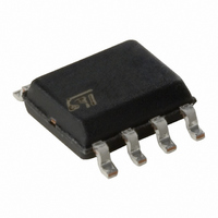
M95040-WMN6T STMicroelectronics, M95040-WMN6T Datasheet - Page 8

M95040-WMN6T
Manufacturer Part Number
M95040-WMN6T
Description
IC EEPROM 4KBIT 10MHZ 8SOIC
Manufacturer
STMicroelectronics
Datasheet
1.M95010-WMN6TP.pdf
(43 pages)
Specifications of M95040-WMN6T
Format - Memory
EEPROMs - Serial
Memory Type
EEPROM
Memory Size
4K (512 x 8)
Speed
10MHz
Interface
SPI, 3-Wire Serial
Voltage - Supply
2.5 V ~ 5.5 V
Operating Temperature
-40°C ~ 85°C
Package / Case
8-SOIC (3.9mm Width)
Lead Free Status / RoHS Status
Contains lead / RoHS non-compliant
Other names
497-1945-2
Available stocks
Company
Part Number
Manufacturer
Quantity
Price
Part Number:
M95040-WMN6TP
Manufacturer:
ST
Quantity:
20 000
Part Number:
M95040-WMN6TP/S
Manufacturer:
ST
Quantity:
20 000
Signal description
2
2.1
2.2
2.3
2.4
2.5
8/43
Signal description
During all operations, V
V
All of the input and output signals can be held high or low (according to voltages of V
V
Serial Data output (Q)
This output signal is used to transfer data serially out of the device. Data is shifted out on the
falling edge of Serial Clock (C).
Serial Data input (D)
This input signal is used to transfer data serially into the device. It receives instructions,
addresses, and the data to be written. Values are latched on the rising edge of Serial Clock
(C).
Serial Clock (C)
This input signal provides the timing of the serial interface. Instructions, addresses, or data
present at Serial Data Input (D) are latched on the rising edge of Serial Clock (C). Data on
Serial Data Output (Q) changes after the falling edge of Serial Clock (C).
Chip Select (S)
When this input signal is high, the device is deselected and Serial Data Output (Q) is at high
impedance. Unless an internal Write cycle is in progress, the device will be in the Standby
Power mode. Driving Chip Select (S) low selects the device, placing it in the Active Power
mode.
After Power-up, a falling edge on Chip Select (S) is required prior to the start of any
instruction.
Hold (HOLD)
The Hold (HOLD) signal is used to pause any serial communications with the device without
deselecting the device.
During the Hold condition, the Serial Data Output (Q) is high impedance, and Serial Data
Input (D) and Serial Clock (C) are Don’t Care.
To start the Hold condition, the device must be selected, with Chip Select (S) driven low.
CC
IL
or V
(min) to V
OL
, as specified in
CC
(max).
CC
Table 13
must be held stable and within the specified valid range:
Doc ID 6512 Rev 8
to
Table
16). These signals are described next.
M95040, M95020, M95010
IH
, V
OH
,


