CY62128VLL-70SC Cypress Semiconductor Corp, CY62128VLL-70SC Datasheet

IC SRAM 1MBIT 70NS 32SOIC

CY62128VLL-70SC

Manufacturer Part Number
CY62128VLL-70SC
Description
IC SRAM 1MBIT 70NS 32SOIC
Manufacturer
Cypress Semiconductor Corp
Datasheet

Specifications of CY62128VLL-70SC

Format - Memory
RAM
Memory Type
SRAM
Memory Size
1M (128K x 8)
Speed
70ns
Interface
Parallel
Voltage - Supply
2.7 V ~ 3.6 V
Operating Temperature
0°C ~ 70°C
Package / Case
32-SOIC (11.30mm Width)
Lead Free Status / RoHS Status
Contains lead / RoHS non-compliant
Other names
428-1073

Available stocks

Company
Part Number
Manufacturer
Quantity
Price
Part Number:
CY62128VLL-70SC
Manufacturer:
CYPRESS
Quantity:
1 200
Part Number:
CY62128VLL-70SC
Manufacturer:
CY
Quantity:
5 530
Part Number:
CY62128VLL-70SC
Manufacturer:
CYPRESS/赛普拉斯
Quantity:
20 000
Features
Functional Description
The CY62128V family is composed of three high-performance
CMOS static RAMs organized as 131,072 words by 8 bits.
Easy memory expansion is provided by an active LOW Chip
Enable (CE
Cypress Semiconductor Corporation
• Low voltage range:
• Low active power and standby power
• Easy memory expansion with CE and OE features
• TTL-compatible inputs and outputs
• Automatic power-down when deselected
• CMOS for optimum speed/power
Logic Block Diagram
CE
CE
WE
OE
— 2.7V–3.6V (CY62128V)
— 2.3V–2.7V (CY62128V25)
— 1.6V–2.0V (CY62128V18)
1
2
A
A
A
A
A
A
A
A
A
V
CE
0
1
2
3
4
5
6
7
8
A
A
A
A
WE
A
A
NC
CC
A
A
A
A
A
A
12
14
16
15
13
11
4
5
6
7
2
8
9
1
16
15
14
13
12
11
10
9
8
7
6
5
4
3
2
1
), an active HIGH Chip Enable (CE
Reverse TSOP I
INPUT BUFFER
(not to scale)
512x 256x 8
Top View
DECODER
COLUMN
ARRAY
POWER
DOWN
17
18
19
20
21
22
23
24
25
26
27
28
29
30
31
32
A
A
A
A
I/O
I/O
I/O
GND
I/O
I/O
I/O
I/O
I/O
CE
A
OE
3
2
1
0
10
0
1
2
3
4
5
6
7
1
3901 North First Street
2
), an active
CE
V
WE
A
A
A
NC
A
A
A
CC
A
A
A
A
A
A
11
13
15
16
14
12
9
8
2
7
6
5
4
62128V-1
25
26
27
26
28
29
30
31
32
1
2
3
4
5
6
7
8
62128V-3
I/O
I/O
I/O
I/O
I/O
I/O
I/O
I/O
0
1
2
3
4
5
6
7
(not to scale)
Top View
STSOP
LOW Output Enable (OE) and three-state drivers. These de-
vices have an automatic power-down feature, reducing the
power consumption by over 99% when deselected. The
CY62128V family is available in the standard 450-mil-wide
SOIC, 32-lead TSOP-I, and STSOP packages.
Writing to the device is accomplished by taking Chip Enable
one (CE
Enable two (CE
through I/O
address pins (A
Reading from the device is accomplished by taking Chip En-
able one (CE
Write Enable (WE) and Chip Enable two (CE
these conditions, the contents of the memory location speci-
fied by the address pins will appear on the I/O pins.
The eight input/output pins (I/O
high-impedance state when the device is deselected (CE
HIGH or CE
during a write operation (CE
1
) and Write Enable (WE) inputs LOW and the Chip
24
23
22
21
20
19
18
17
16
15
14
13
12
11
10
9
7
San Jose
) is then written into the location specified on the
2
1
OE
A
CE
I/O
I/O
I/O
I/O
I/O
GND
I/O
I/O
I/O
A
A
A
A
LOW), the outputs are disabled (OE HIGH), or
10
0
1
2
3
) and Output Enable (OE) LOW while forcing
1
7
6
5
4
3
2
1
0
2
0
) input HIGH. Data on the eight I/O pins (I/O
through A
128K x 8 Static RAM
CE
V
A
A
WE
A
A
A
A
NC
A
A
CC
A
A
A
A
11
13
15
16
14
12
9
8
2
7
6
5
4
Pin Configurations
GND
1
2
3
4
5
6
7
8
9
10
11
12
13
14
15
16
I/O
I/O
I/O
A
A
A
16
NC
1
A
A
A
A
A
A
A
A
16
14
12
6
5
4
3
2
1
0
0
1
2
CY62128V Family
7
CA 95134
LOW, CE
).
0
13
14
15
16
1
2
3
4
5
6
7
8
9
10
11
12
through I/O
Top View
SOIC
(not to scale)
Top View
TSOP I
2
32
31
30
29
28
27
26
25
24
23
22
21
20
19
18
17
HIGH, and WE LOW).
CE
A
CE
I/O
I/O
I/O
I/O
I/O
V
A
WE
A
A
A
A
OE
7
CC
10
15
13
8
9
11
7
6
5
4
3
) are placed in a
2
1
2
March 27, 2001
) HIGH. Under
408-943-2600
62128V-4
62128V-2
32
31
30
29
28
27
26
25
24
23
22
21
20
19
18
17
OE
A
CE
I/O
I/O
I/O
I/O
I/O
GND
I/O
I/O
I/O
A
A
A
A
10
0
1
2
3
1
7
6
5
4
3
2
1
0
0
1

Related parts for CY62128VLL-70SC

CY62128VLL-70SC Summary of contents

Page 1

... Cypress Semiconductor Corporation LOW Output Enable (OE) and three-state drivers. These de- vices have an automatic power-down feature, reducing the power consumption by over 99% when deselected. The CY62128V family is available in the standard 450-mil-wide SOIC, 32-lead TSOP-I, and STSOP packages. Writing to the device is accomplished by taking Chip Enable ...

Page 2

Maximum Ratings (Above which the useful life may be impaired. For user guide- lines, not tested.) Storage Temperature ................................. –65°C to +150°C Ambient Temperature with Power Applied ............................................. –55°C to +125°C Supply Voltage to Ground Potential (Pin 28 to Pin ...

Page 3

Electrical Characteristics Over the Operating Range (continued) Parameter Description I Automatic CE SB2 Power-Down Current— CMOS Inputs Electrical Characteristics Over the Operating Range Parameter Description V Output HIGH Voltage OH V Output LOW Voltage OL V Input HIGH Voltage IH ...

Page 4

AC Test Loads and Waveforms OUTPUT INCLUDING JIG AND 62128V–5 SCOPE Equivalent to: THÉ VENIN EQUIVALENT R TH OUTPUT Parameters 3.3V R1 1213 R2 1378 R 645 TH V 1.75V TH Data Retention Characteristics ...

Page 5

... HZWE L 8. The internal write time of the memory is defined by the overlap of CE write and either signal can terminate a write by going HIGH. The data input set-up and hold timing should be referenced to the rising edge of the signal that terminates the write. 9. The minimum write cycle time for write cycle #3 (WE controlled, OE LOW) is the sum of t (for “ ...

Page 6

Switching Waveforms [10, 11] Read Cycle No. 1 ADDRESS DATA OUT PREVIOUS DATA VALID [11, 12] Read Cycle No. 2 (OE Controlled) ADDRESS ACE OE t LZOE HIGH IMPEDANCE DATA OUT t LZCE t V ...

Page 7

Switching Waveforms (continued) Write Cycle No. 2 (WE Controlled, OE HIGH During Write) ADDRESS DATA I/O NOTE 15 t HZOE Truth Table ...

Page 8

... Ordering Information Speed (ns) Ordering Code 55 CY62128VLL-55ZAI 70 CY62128VL-70SC CY62128VLL-70SC CY62128VL-70ZC CY62128VLL-70ZC CY62128VL-70ZAC CY62128VLL-70ZAC CY62128VLL-70ZRC CY62128VLL-70SI CY62128VL-70ZI CY62128VLL-70ZI CY62128VL-70ZAI CY62128VLL-70ZAI CY62128VLL-70ZRI 200 CY62128V18L-200ZC CY62128V18L-200ZAI CY62128V18LL-200ZAI Document #: 38-00547-*C Package Name Package Type ZA32 32-Lead STSOP Type 1 S34 32-Lead 450-Mil SOIC Z32 32-Lead TSOP Type 1 ...

Page 9

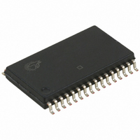
Package Diagrams 32-Lead (450 MIL) Molded SOIC S34 9 CY62128V Family 51-85081-A ...

Page 10

Package Diagrams 32-Lead Thin Small Outline Package Z32 10 CY62128V Family 51-85056-C ...

Page 11

Package Diagrams 32-Lead Shrunk Thin Small Outline Package ZA32 CY62128V Family 11 51-85094-C ...

Page 12

... Reverse Thin Small Outline Package ZR32 © Cypress Semiconductor Corporation, 2001. The information contained herein is subject to change without notice. Cypress Semiconductor Corporation assumes no responsibility for the use of any circuitry other than circuitry embodied in a Cypress Semiconductor product. Nor does it convey or imply any license under patent or other rights. Cypress Semiconductor does not authorize its products for use as critical components in life-support systems where a malfunction or failure may reasonably be expected to result in significant injury to the user ...

Related keywords