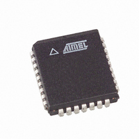
AT49LH00B4-33JC SL383 Atmel, AT49LH00B4-33JC SL383 Datasheet - Page 8

AT49LH00B4-33JC SL383
Manufacturer Part Number
AT49LH00B4-33JC SL383
Description
IC FLASH 4MBIT 33MHZ 32PLCC
Manufacturer
Atmel
Datasheet
1.AT49LH00B4-33JC.pdf
(41 pages)
Specifications of AT49LH00B4-33JC SL383
Format - Memory
FLASH
Memory Type
FLASH
Memory Size
4M (512K x 8)
Speed
33MHz
Interface
Parallel
Voltage - Supply
3 V ~ 3.6 V
Operating Temperature
0°C ~ 85°C
Package / Case
32-PLCC
Lead Free Status / RoHS Status
Contains lead / RoHS non-compliant
7.1
7.2
7.3
8
FWH4/LFRAME Pin
FWH/LAD[3:0] Pins
FWH Memory Cycles
AT49LH00B4
the type of FWH/LPC cycle that is to be performed. The value of the START field determines
whether the device will operate using a FWH cycle or an LPC cycle.
valid START fields that the device will recognize.
Table 7-1.
If a valid START value is not detected, then the device will enter standby mode when the
FWH4/LFRAME pin is high and no internal operation is in progress. The FWH/LAD[3:0] pins will
also be placed in a high-impedance state.
FWH4/LFRAME is used by the master to indicate the start of cycles and the termination of
cycles due to an abort or time-out condition. This signal is to be used by peripherals to know
when to monitor the bus for a cycle.
The FWH4/LFRAME signal is used as a general notification that the FWH/LAD[3:0] lines contain
information relative to the start or stop of a cycle, and that peripherals must monitor the bus to
determine whether the cycle is intended for them. The benefit to peripherals of FWH4/LFRAME
is that it allows them to enter lower power states internally when a cycle is not intended for them.
When peripherals sample FWH4/LFRAME is active, they are to immediately stop driving the
FWH/LAD[3:0] signal lines on the next clock and monitor the bus for new cycle information.
The FWH/LAD[3:0] signal lines communicate address, control, and data information over the
LPC bus between a master and a peripheral. The information communicated are: start, stop
(abort a cycle), transfer type (memory, I/O, DMA), transfer direction (read/write), address, data,
wait states, DMA channel, and bus master grant.
A valid FWH memory cycle begins with the host driving the FWH4/LFRAME signal low for one or
more clock cycles. While the FWH4/LFRAME signal is low, a valid START value of either 1101b
(FWH memory read) or 1110b (FWH memory write) must be driven on the FWH/LAD[3:0] pins.
Following the START field, an IDSEL (Device Select) field must be sent to the device. The
IDSEL field acts like a chip select in that it indicates which device should respond to the current
operation. After the IDSEL field has been sent, the 7-clock MADDR (Memory Address) field
must be sent to the device to provide the 28-bit starting address location of where to begin read-
ing or writing in the memory. Following the MADDR field, the MSIZE (Memory Size) field must
be sent to indicate the number of bytes to transfer.
START Value
0000b
1101b
1110b
FWH/LPC Start Fields
Cycle Type
LPC Cycle – The type (memory, I/O, DMA) and direction of the cycle (read or write)
is determined by the second field (CYCTYPE + DIR) of the LPC cycle. Only memory
cycles are supported by the device.
FWH Memory Read Cycle
FWH Memory Write Cycle
Table 7-1
details the three
3379C–FLASH–3/05


