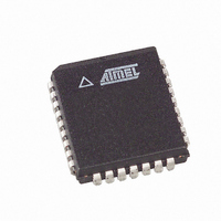
AT49LH00B4-33JC Atmel, AT49LH00B4-33JC Datasheet - Page 20

AT49LH00B4-33JC
Manufacturer Part Number
AT49LH00B4-33JC
Description
IC FLASH 4MBIT 33MHZ 32PLCC
Manufacturer
Atmel
Datasheet
1.AT49LH00B4-33JC.pdf
(41 pages)
Specifications of AT49LH00B4-33JC
Format - Memory
FLASH
Memory Type
FLASH
Memory Size
4M (512K x 8)
Speed
33MHz
Interface
Parallel
Voltage - Supply
3 V ~ 3.6 V
Operating Temperature
0°C ~ 85°C
Package / Case
32-PLCC
Lead Free Status / RoHS Status
Contains lead / RoHS non-compliant
Available stocks
Company
Part Number
Manufacturer
Quantity
Price
Company:
Part Number:
AT49LH00B4-33JC
Manufacturer:
ATMEL
Quantity:
975
11.2
20
Register-Based Sector Locking
AT49LH00B4
Table 11-1.
The TBL and WP pins must be set to the desired protection state prior to starting a program or
erase operation because they are sampled at the beginning of the operation. Changing the state
of TBL or WP during a program or erase operation may cause unpredictable results. The new
lock status will take place after the program or erase operation completes.
The TBL and WP pins function independently from the Sector Locking Registers. These pins,
when active, will write protect the appropriate sector(s) against program and erase operations
regardless of the values of the Sector Locking Registers. For example, when TBL is active, writ-
ing to the top sector is prevented regardless of the state of the Write-Lock bit for the top sector’s
locking register. In such a case, clearing the Write-Lock bit in the Sector Locking Register will
have no functional effect even though the register may indicate that the sector is no longer
locked. However, the register may still be set to Read-Lock the sector if desired.
For protecting the sectors of the memory array, the TBL and WP pins always take precedence
over the Sector Locking Registers. In addition, the states of the TBL and WP pins have no effect
on the values or status of the Sector Locking Registers.
The device has eleven Sector Locking Registers that are used in lieu of or in conjunction with
the TBL and WP pins to control the lock protection for each sector in the memory array. The
Sector Locking Registers are accessed through their respective address locations (detailed in
Table
memory and register accesses differs when the device is used as a FWH or LPC Flash (A22 for
FWH and A23 for LPC), the register memory address will also differ.
The Sector Locking Registers are both readable and writable, and each register has three dedi-
cated locking bits to control Read Lock, Write Lock, and Lock Down functions. Therefore, a
Sector Locking Register can be read to determine what its current value is set to (e.g., set to
Lock Down status). Reading the Sector Locking Registers, however, will not determine the sta-
tus of the TBL and WP pins.
When returning from a reset condition or after power-up, the Sector Locking Registers will
always default to a state of 01H.
Sector
11-2) in the 4 GB system memory map. Since the address bit used to distinguish between
10
9
8
7
6
5
4
3
2
1
0
Hardware Write Protection Options
Size (Bytes)
64K
64K
64K
64K
64K
64K
64K
32K
16K
8K
8K
070000H - 07FFFFH
060000H - 06FFFFH
050000H - 05FFFFH
040000H - 04FFFFH
030000H - 03FFFFH
020000H - 02FFFFH
010000H - 01FFFFH
008000H - 00FFFFH
004000H - 007FFFH
002000H - 003FFFH
000000H - 001FFFH
Address Range
Hardware Write Protection
TBL
WP
WP
WP
WP
WP
WP
WP
WP
WP
WP
3379C–FLASH–3/05


