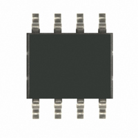
M25P40-VMN6TPB NUMONYX, M25P40-VMN6TPB Datasheet - Page 19

M25P40-VMN6TPB
Manufacturer Part Number
M25P40-VMN6TPB
Description
IC FLASH 4MBIT 75MHZ 8SOIC
Manufacturer
NUMONYX
Series
Forté™r
Datasheet
1.M25P40-VMP6G.pdf
(61 pages)
Specifications of M25P40-VMN6TPB
Format - Memory
FLASH
Memory Type
FLASH
Memory Size
4M (512K x 8)
Speed
75MHz
Interface
SPI, 3-Wire Serial
Voltage - Supply
2.3 V ~ 3.6 V
Operating Temperature
-40°C ~ 85°C
Package / Case
8-SOIC (3.9mm Width)
Lead Free Status / RoHS Status
Lead free / RoHS Compliant
Other names
M25P40-VMN6TPBTR
Available stocks
Company
Part Number
Manufacturer
Quantity
Price
Company:
Part Number:
M25P40-VMN6TPB
Manufacturer:
MICRON
Quantity:
21 000
Company:
Part Number:
M25P40-VMN6TPB
Manufacturer:
MICRON
Quantity:
11 200
Company:
Part Number:
M25P40-VMN6TPB
Manufacturer:
Numonyx
Quantity:
22 500
Company:
Part Number:
M25P40-VMN6TPB
Manufacturer:
MICRON44
Quantity:
18 188
Part Number:
M25P40-VMN6TPB
Manufacturer:
MICRON
Quantity:
20 000
6.1
Table 4.
1. The Read Identification (RDID) instruction is available only for parts made with 110 nm Technology
Write Enable (WREN)
The Write Enable (WREN) instruction
The Write Enable Latch (WEL) bit must be set prior to every Page Program (PP), Sector
Erase (SE), Bulk Erase (BE) and Write Status Register (WRSR) instruction.
The Write Enable (WREN) instruction is entered by driving Chip Select (S) Low, sending the
instruction code, and then driving Chip Select (S) High.
Figure 7.
FAST_READ
Instruction
identified with Process letter '4'. (Also, see Application Note AN1995).
RDID
WREN
WRSR
RDSR
READ
WRDI
RES
DP
PP
SE
BE
(1)
Instruction set
Write Enable (WREN) instruction sequence
Write Enable
Write Disable
Read Identification
Read Status Register
Write Status Register
Read Data Bytes
Read Data Bytes at Higher
Speed
Page Program
Sector Erase
Bulk Erase
Deep Power-down
Release from Deep Power-
down, and Read Electronic
Signature
Release from Deep Power-
down
S
C
D
Q
Description
High Impedance
0
(Figure
1
One-byte instruction
2
0000 0100
0000 0101
0000 0001
0000 0010
Instruction
0000 0110
0000 0011
0000 1011
1101 1000
1011 1001
1010 1011
1001 1111
1100 0111
3
7) sets the Write Enable Latch (WEL) bit.
4
code
5
6
7
D8h
C7h
ABh
9Fh
0Bh
B9h
06h
04h
05h
01h
03h
02h
Address
AI02281E
bytes
0
0
0
0
0
3
3
3
3
0
0
0
0
Dummy
bytes
0
0
0
0
0
0
1
0
0
0
0
3
0
1 to 256
1 to ∞
1 to ∞
1 to ∞
1 to ∞
bytes
1 to 3
Data
0
0
1
0
0
0
0
19/61


