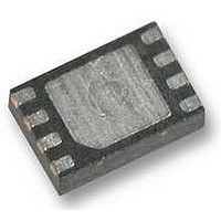
M25P20-VMP6G NUMONYX, M25P20-VMP6G Datasheet - Page 41

M25P20-VMP6G
Manufacturer Part Number
M25P20-VMP6G
Description
IC FLASH 2MBIT 50MHZ 8VFQFPN
Manufacturer
NUMONYX
Series
Forté™r
Specifications of M25P20-VMP6G
Format - Memory
FLASH
Memory Type
FLASH
Memory Size
2M (256K x 8)
Speed
50MHz
Interface
SPI, 3-Wire Serial
Voltage - Supply
2.7 V ~ 3.6 V
Operating Temperature
-40°C ~ 85°C
Package / Case
8-VFQFN, 8-VFQFPN
Clock Frequency
50MHz
Supply Voltage Range
2.7V To 3.6V
Memory Case Style
VDFPN
No. Of Pins
8
Base Number
25
Frequency
50MHz
Ic Generic Number
25P20
Memory Configuration
256K X 8
Interface Type
Serial, SPI
Rohs Compliant
Yes
Lead Free Status / RoHS Status
Lead free / RoHS Compliant
Available stocks
Company
Part Number
Manufacturer
Quantity
Price
Company:
Part Number:
M25P20-VMP6G
Manufacturer:
Micron Technology Inc
Quantity:
10 000
Part Number:
M25P20-VMP6G
Manufacturer:
ST
Quantity:
20 000
Company:
Part Number:
M25P20-VMP6GB
Manufacturer:
MICRON
Quantity:
5 600
M25P20
Table 19.
1. Details of how to find the date of marking are given in Application Note, AN1995.
2. t
3. Value guaranteed by characterization, not 100% tested in production.
4. Expressed as a slew-rate.
5. Only applicable as a constraint for a WRSR instruction when SRWD is set at 1.
6. It is 30µs in devices produced with the “X” process technology. Details of how to find the process letter on
Symbol
t
t
t
t
t
t
t
t
t
HHQX
WHSL
SHWL
CLCH
CHCL
SHQZ
HLQZ
RES1
RES2
t
t
t
t
t
t
t
t
t
t
t
t
t
t
t
t
CH
CHHH
HHCH
DVCH
CHDX
CHSH
SHCH
CLQV
CLQX
HLCH
CHHL
SLCH
CHSL
SHSL
DP
CL
the device marking are given in the Application note AN1995.
CH
f
f
C
R
(2)
(3)
(2)
(3)
(3)
(3)
(3)
(3)
+ t
(3)
(3)
(5)
(5)
CL
must be greater than or equal to 1/ f
t
t
t
t
t
AC Characteristics (40MHz Operation, Device Grade 6)
Alt.
t
DSU
t
CSH
t
CLH
CSS
t
40MHz available for products marked since week 20 of 2004, only
CLL
t
DIS
HO
f
DH
t
HZ
LZ
C
V
Clock Frequency for the following
instructions: FAST_READ, PP, SE, BE,
DP, RES, WREN, WRDI, RDSR, WRSR
Clock Frequency for READ instructions
Clock High Time
Clock Low Time
Clock Rise Time
Clock Fall Time
S Active Setup Time (relative to C)
S Not Active Hold Time (relative to C)
Data In Setup Time
Data In Hold Time
S Active Hold Time (relative to C)
S Not Active Setup Time (relative to C)
S Deselect Time
Output Disable Time
Clock Low to Output Valid
Output Hold Time
HOLD Setup Time (relative to C)
HOLD Hold Time (relative to C)
HOLD Setup Time (relative to C)
HOLD Hold Time (relative to C)
HOLD to Output Low-Z
HOLD to Output High-Z
Write Protect Setup Time
Write Protect Hold Time
S High to Deep Power-down Mode
S High to Standby Mode without
Electronic Signature Read
S High to Standby Mode with Electronic
Signature Read
Test conditions specified in
Parameter
(4)
(4)
(peak to peak)
(peak to peak)
C
Table 10
and
Min.
D.C.
D.C.
100
100
0.1
0.1
11
11
20
5
5
5
2
5
5
0
5
5
5
5
Table 17
Typ.
DC and AC parameters
1.8 or 30
3 or 30
(1)
Max.
40
20
9
9
9
9
3
(6)
(6)
MHz
Unit
MHz
V/ns
V/ns
41/50
ns
ns
ns
ns
ns
ns
ns
ns
ns
ns
ns
ns
ns
ns
ns
ns
ns
ns
ns
ns
μs
μs
μs


