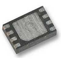
M25P20-VMP6G NUMONYX, M25P20-VMP6G Datasheet - Page 12

M25P20-VMP6G
Manufacturer Part Number
M25P20-VMP6G
Description
IC FLASH 2MBIT 50MHZ 8VFQFPN
Manufacturer
NUMONYX
Series
Forté™r
Specifications of M25P20-VMP6G
Format - Memory
FLASH
Memory Type
FLASH
Memory Size
2M (256K x 8)
Speed
50MHz
Interface
SPI, 3-Wire Serial
Voltage - Supply
2.7 V ~ 3.6 V
Operating Temperature
-40°C ~ 85°C
Package / Case
8-VFQFN, 8-VFQFPN
Clock Frequency
50MHz
Supply Voltage Range
2.7V To 3.6V
Memory Case Style
VDFPN
No. Of Pins
8
Base Number
25
Frequency
50MHz
Ic Generic Number
25P20
Memory Configuration
256K X 8
Interface Type
Serial, SPI
Rohs Compliant
Yes
Lead Free Status / RoHS Status
Lead free / RoHS Compliant
Available stocks
Company
Part Number
Manufacturer
Quantity
Price
Company:
Part Number:
M25P20-VMP6G
Manufacturer:
Micron Technology Inc
Quantity:
10 000
Part Number:
M25P20-VMP6G
Manufacturer:
ST
Quantity:
20 000
Company:
Part Number:
M25P20-VMP6GB
Manufacturer:
MICRON
Quantity:
5 600
Operating features
4.5
4.6
12/50
Status Register
The Status Register contains a number of status and control bits, as shown in
can be read or set (as appropriate) by specific instructions. For a detailed description of the
Status Register bits, see
Protection Modes
The environments where non-volatile memory devices are used can be very noisy. No SPI
device can operate correctly in the presence of excessive noise. To help combat this, the
M25P20 features the following data protection mechanisms:
●
●
●
●
●
●
Power On Reset and an internal timer (t
changes while the power supply is outside the operating specification.
Program, Erase and Write Status Register instructions are checked that they consist of
a number of clock pulses that is a multiple of eight, before they are accepted for
execution.
All instructions that modify data must be preceded by a Write Enable (WREN)
instruction to set the Write Enable Latch (WEL) bit. This bit is returned to its reset state
by the following events:
–
–
–
–
–
–
The Block Protect (BP1, BP0) bits allow part of the memory to be configured as read-
only. This is the Software Protected Mode (SPM).
The Write Protect (W) signal, in co-operation with the Status Register Write Disable
(SRWD) bit, allows the Block Protect (BP1, BP0) bits and Status Register Write Disable
(SRWD) bit to be write-protected. This is the Hardware Protected Mode (HPM).
In addition to the low power consumption feature, the Deep Power-down mode offers
extra software protection from inadvertant Write, Program and Erase instructions, as all
instructions are ignored except one particular instruction (the Release from Deep
Power-down instruction).
Power-up
Write Disable (WRDI) instruction completion
Write Status Register (WRSR) instruction completion
Page Program (PP) instruction completion
Sector Erase (SE) instruction completion
Bulk Erase (BE) instruction completion
Section 6.4: Read Status Register
PUW
) can provide protection against inadvertant
(RDSR).
Table
M25P20
6, that


