AT34C02C-TH-T Atmel, AT34C02C-TH-T Datasheet
AT34C02C-TH-T
Specifications of AT34C02C-TH-T
Available stocks


Related parts for AT34C02C-TH-T


AT34C02C-TH-T Summary of contents
Page 1
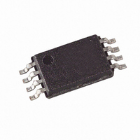
... The device is optimized for use in many industrial and commercial applications where low-power and low-voltage operations are essential. The AT34C02C is available in space saving 8-lead JEDEC SOIC, , 8-lead TSSOP, and 8-ball dBGA2 packages and is accessed via a Two- Mini-MAP (MLP 2x3) wire serial interface ...
Page 2
... Figure 1-1. Block diagram V CC GND WP START SCL STOP SDA LOGIC ADDRESS COMPARATOR Atmel AT34C02C 2 *NOTICE: SERIAL CONTROL LOGIC WRITE PROTECT CIRCUITRY LOAD COMP DEVICE LOAD INC R/W DATA WORD ADDR/COUNTER Y DEC D OUT Stresses beyond those listed under “Absolute Maximum Ratings” may cause permanent dam- age to the device ...
Page 3
... GND. However, due to capacitive coupling that may appear during customer applications, Atmel recommends always connecting the WP pins to a known state. When using a pull-up resistor, Atmel recommends using 10k or less. Table 2-1. Atmel AT34C02C write protection modes WP pin status V CC ...
Page 4
... Inputs fall time F t Stop set-up time SU.STO t Data out hold time DH t Write cycle time WR (1) Endurance 25C, page mode Note: 1. This parameter is characterized and is not 100% tested. Atmel AT34C02C 4 = –40°C to +85° Test Condition READ at 100kHz WRITE at 100kHz ...
Page 5
... Memory organization Atmel AT34C02C, 2K Serial EEPROM: The 2K is internally organized with 16 pages of 16 bytes each. Random word addressing requires a 8-bit data word address. 4. Device operation CLOCK and DATA TRANSITIONS: The SDA pin is normally pulled high with an external device. Data on the SDA pin may change only during SCL low time periods (see a start or stop condition as defined below ...
Page 6
... SCL SDA 8th BIT WORDn Note: 1. The write cycle time t cycle. Figure 4-3. Data validity Figure 4-4. Start and stop condition Atmel AT34C02C 6 ACK ( STOP CONDITION is the time from a valid stop condition of a write sequence to the end of the internal clear/write WR START CONDITION 5185E– ...
Page 7
... The device address word consists of a mandatory one-zero sequence for the first four most-significant bits (1010) for normal read and write operations and 0110 for writing to the write protect register. The next three bits are the A2, A1, and A0 device address bits for the Atmel AT34C02C EEPROM. These three bits must compare to their corresponding hard-wired input pins. ...
Page 8
... WP pin is connected GND or left floating, the write protection mode is determined by the status of the software write protect register. Figure 7-1. Setting permanent write protect register (PSWP) S CONTROL T A BYTE R T SDA LINE Atmel AT34C02C 8 connected to VHV (see 0 Figure 7-3). WORD ADDRESS DATA ...
Page 9
... Write protection Command A2 Set PSWP A2 Set RSWP 0 Clear RSWP 0 Table 7-2. VHV VHV Note: VHV - V > 4.8V CC 5185E–SEEPR–3/11 WORD ADDRESS DATA Don't Care WORD ADDRESS DATA Don't Care Pin VHV VHV 0 1 Min Max 7 10 Atmel AT34C02C Preamble Units ...
Page 10
... Not programmed Read RSWP R X Read RSWP R X Set RSWP W X Set RSWP W X Clear RSWP W Programmed Clear RSWP W Not programmed Atmel AT34C02C 10 Reversible write protect register Acknowledgment RSWP from device X ACK X ACK Programmed ACK Not programmed ACK X No ACK X ACK ...
Page 11
... No ACK Not programmed ACK X No ACK X ACK Figure 8-4 on page Atmel AT34C02C Action from device Read array Device write protect STOP - Indicates permanent write protect register is programmed Read out data don't care. Indicates PSWP register is not programmed STOP - Indicates permanent write protect register is ...
Page 12
... Otherwise, it has been programmed and the device is write protected (reversible) at the first half of the array. Figure 8-1. Device address Figure 8-2. Byte write Figure 8-3. Page write Atmel AT34C02C 12 13). Pin ...
Page 13
... Figure 8-4. Current address read Figure 8-5. Random read Figure 8-6. Sequential read 5185E–SEEPR–3/11 Atmel AT34C02C 13 ...
Page 14
... AT34C02CN-SH-B (NiPdAu lead finish) (2) AT34C02CN-SH-T (NiPdAu lead finish) (1) AT34C02C-TH-B (NiPdAu lead finish) (2) AT34C02C-TH-T (NiPdAu lead finish) (2) AT34C02CY6-YH-T (NiPdAu lead finish) (2) AT34C02CU3-UU-T Notes: 1. “-B” denotes bulk 2. “-T” denotes tape and reel. SOIC = 4K per reel; TSSOP, Ultra Thin Mini MAP and dBGA2 = 5K per reel. ...
Page 15
... B: February 04: Week 4 “ ” “ ” “ ” L: December 52: Week 52 TITLE 34C02CSM, AT34C02C Standard Marking Information for Package Offering Atmel AT34C02C 8 lead SOIC 3 Rows of 8 Characters ATMLHYWW 34C1 AAAAAAAA 8 lead UDFN - 2.0x3.0mm 3 Rows of 3 Characters 34C H1@ YXX PIN 1 Catalog Truncation: 34C ...
Page 16
... JEDEC SOIC TOP VIEW TOP VIEW e e SIDE VIEW SIDE VIEW Notes: This drawing is for general information only. Refer to JEDEC Drawing MS-012, Variation AA for proper dimensions, tolerances, datums, etc. Package Drawing Contact: packagedrawings@atmel.com Atmel AT34C02C TITLE 8S1, 8-lead (0.150” Wide Body), Plastic Gull ...
Page 17
... Minimum space between protrusion and adjacent lead is 0.07mm. 5. Dimension D and determined at Datum Plane H. Package Drawing Contact: packagedrawings@atmel.com 5185E–SEEPR–3/ TITLE 8A2, 8-lead 4.4mm Body, Plastic Thin Shrink Small Outline Package (TSSOP) Atmel AT34C02C L1 L End View COMMON DIMENSIONS (Unit of Measure = mm) MIN MAX SYMBOL NOM D 2.90 3 ...
Page 18
... Soldering the large thermal pad is optional, but not recommended. No electrical connection is accomplished to the device through this pad soldered it should be tied to ground Package Drawing Contact: packagedrawings@atmel.com Atmel AT34C02C 18 A Pin 1 Index Area A2 A3 TITLE 8Y6, 8-lead, 2 ...
Page 19
... E D PIN 1 BALL PAD CORNER TOP VIEW (d1 (e1) BOTTOM VIEW 8 SOLDER BALLS TITLE 8U3-1, 8-ball, 1.50 x 2.00 mm Body, 0.50 pitch, VFBGA Package (dBGA2) Atmel AT34C02C SIDE VIEW COMMON DIMENSIONS (Unit of Measure - mm) SYMBOL MIN NOM MAX NOTE A 0.73 0.79 0.85 A1 0.09 ...
Page 20
... Revision history Doc. rev. Date 5185E 03/2011 5185D 01/2008 5185C 08/2007 5185B 03/2007 Atmel AT34C02C 20 Comments Replaced part markings to single page part markings Updated template Removed ‘preliminary’ status Updated to new template Added package marking tables Implemented revision history 5185E–SEEPR–3/11 ...
Page 21
... Disclaimer: The information in this document is provided in connection with Atmel products. No license, express or implied, by estoppel or otherwise, to any intellectual property right is granted by this document or in connection with the sale of Atmel products. EXCEPT AS SET FORTH IN THE ATMEL TERMS AND CONDITIONS OF SALES LOCATED ON THE ATMEL WEBSITE, ATMEL ASSUMES NO LIABILITY WHATSOEVER AND DISCLAIMS ANY EXPRESS, IMPLIED OR STATUTORY WARRANTY RELATING TO ITS PRODUCTS INCLUDING, BUT NOT LIMITED TO, THE IMPLIED WARRANTY OF MERCHANTABILITY, FITNESS FOR A PARTICULAR PURPOSE, OR NON-INFRINGEMENT ...