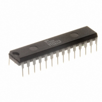
IDT71256SA20TPG IDT, Integrated Device Technology Inc, IDT71256SA20TPG Datasheet - Page 3

IDT71256SA20TPG
Manufacturer Part Number
IDT71256SA20TPG
Description
IC SRAM 256KBIT 20NS 28DIP
Manufacturer
IDT, Integrated Device Technology Inc
Datasheet
1.IDT71256SA12YG8.pdf
(8 pages)
Specifications of IDT71256SA20TPG
Format - Memory
RAM
Memory Type
SRAM
Memory Size
256K (32K x 8)
Speed
20ns
Interface
Parallel
Voltage - Supply
4.5 V ~ 5.5 V
Operating Temperature
0°C ~ 70°C
Package / Case
28-DIP (0.300", 7.62mm)
Density
256Kb
Access Time (max)
20ns
Sync/async
Asynchronous
Architecture
Not Required
Clock Freq (max)
Not RequiredMHz
Operating Supply Voltage (typ)
5V
Address Bus
15b
Package Type
PDIP
Operating Temp Range
0C to 70C
Number Of Ports
1
Supply Current
145mA
Operating Supply Voltage (min)
4.5V
Operating Supply Voltage (max)
5.5V
Operating Temperature Classification
Commercial
Mounting
Through Hole
Pin Count
28
Word Size
8b
Number Of Words
32K
Lead Free Status / RoHS Status
Lead free / RoHS Compliant
Other names
71256SA20TPG
800-1430
800-1430-5
800-1430
800-1430
800-1430-5
800-1430
Available stocks
Company
Part Number
Manufacturer
Quantity
Price
DC Electrical Characteristics
(V
DC Electrical Characteristics
(V
NOTES:
1. All values are maximum guaranteed values.
2. f
AC Test Conditions
Input Pulse Levels
Input Rise/Fall Times
Input Timing Reference Levels
Output Reference Levels
AC Test Load
IDT71256SA
CMOS Static RAM 256K (32K x 8-Bit)
Symbol
CC
CC
Symbol
MAX
I
I
I
SB1
CC
SB
V
V
|I
|I
LO
OH
LI
OL
= 5.0V ± 10%)
= 1/t
= 5.0V ± 10%, V
|
|
DATA
RC
Dynamic Operating Current
Standby Power Supply Current (TTL Level)
Standby Power Supply Current (CMOS Level)
CS < V
CS > V
CS > V
V
(all address inputs are cycling at f
IN
Input Leakage Current
Output Leakage Current
Output Low Voltage
Output High Voltage
< V
OUT
30pF*
IL
IH
HC
LC
, Outputs Open, V
, Outputs Open, V
, Outputs Open, V
or V
Figure 1. AC Test Load
IN
Parameter
> V
LC
HC
Parameter
= 0.2V, V
CC
CC
CC
= Max., f = f
5V
= Max., f = f
= Max., f = 0
MAX
480Ω
255Ω
See Figures 1 and 2
); f = 0 means no address input lines are changing.
2948 drw 03
HC
GND to 3.0V
I
I
V
V
OL
OH
MAX
MAX
CC
CC
(2)
1.5V
1.5V
= V
= 8mA, V
3ns
= -4mA, V
*Including jig and scope capacitance.
(2)
,
= Max., V
= Max., CS = V
(2)
(1)
,
CC
2948 tbl 07
–0.2V)
CC
CC
IN =
71256SA12
= Min.
= Min.
GND to V
6.42
160
50
15
IH
3
, V
Test Conditions
NOTE:
1. This parameter is guaranteed by device characterization, but not production
Capacitance
(T
C
C
OUT
IN
I/O
Symbol
A
tested.
CC
= GND to V
= +25°C, f = 1.0MHz, SOJ package)
DATA
71256SA15
Input Capacitance
I/O Capacitance
150
40
15
CC
OUT
Commercial and Industrial Temperature Ranges
(for t
5pF*
Parameter
CLZ
Figure 2. AC Test Load
, t
OLZ
(1)
71256SA20
, t
CHZ
145
40
15
, t
OHZ
5V
, t
V
Conditions
V
Min.
OUT
2.4
OW,
___
___
___
IN
480Ω
255Ω
IDT71256SA
= 3dV
2948 drw 04
= 3dV
and t
71256SA25
WHZ
145
40
15
Max.
)
0.4
___
5
5
Max.
.
7
7
2948 tbl 05
2948 tbl 06
2948 tbl 08
Unit
µ A
µ A
Unit
Unit
mA
mA
mA
V
V
pF
pF


