IDT71256SA20TPG IDT, Integrated Device Technology Inc, IDT71256SA20TPG Datasheet - Page 2
IDT71256SA20TPG
Manufacturer Part Number
IDT71256SA20TPG
Description
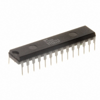
IC SRAM 256KBIT 20NS 28DIP
Manufacturer
IDT, Integrated Device Technology Inc
Datasheet
1.IDT71256SA12YG8.pdf
(8 pages)
Specifications of IDT71256SA20TPG
Format - Memory
RAM
Memory Type
SRAM
Memory Size
256K (32K x 8)
Speed
20ns
Interface
Parallel
Voltage - Supply
4.5 V ~ 5.5 V
Operating Temperature
0°C ~ 70°C
Package / Case
28-DIP (0.300", 7.62mm)
Density
256Kb
Access Time (max)
20ns
Sync/async
Asynchronous
Architecture
Not Required
Clock Freq (max)
Not RequiredMHz
Operating Supply Voltage (typ)
5V
Address Bus
15b
Package Type
PDIP
Operating Temp Range
0C to 70C
Number Of Ports
1
Supply Current
145mA
Operating Supply Voltage (min)
4.5V
Operating Supply Voltage (max)
5.5V
Operating Temperature Classification
Commercial
Mounting
Through Hole
Pin Count
28
Word Size
8b
Number Of Words
32K
Lead Free Status / RoHS Status
Lead free / RoHS Compliant
Other names
71256SA20TPG
800-1430
800-1430-5
800-1430
800-1430
800-1430-5
800-1430
Available stocks
Company
Part Number
Manufacturer
Quantity
Price


Pin Configurations
Recommended Operating
Temperature and Supply Voltage
Commercial
Industrial
IDT71256SA
CMOS Static RAM 256K (32K x 8-Bit)
V
A
A
A
A
WE
OE
CC
A
A
A
A
A
A
A
11
13
14
12
9
8
7
6
5
4
3
Grade
22
23
24
25
26
27
28
1
2
3
4
5
6
7
GND
I/O
I/O
I/O
A
A
A
A
A
A
A
A
A
A
14
12
7
6
5
4
3
2
1
0
0
1
2
-40
Temperature
0
10
11
12
13
14
O
1
2
3
4
5
6
7
8
9
Top View
Top View
C to +70
O
DIP/SOJ
C to +85
SO28-5
TSOP
P28-2
P28-1
SO28-8
O
C
O
C
28
27
26
25
24
23
22
21
20
19
18
17
16
15
2948 drw 02
GND
0V
0V
V
WE
A
A
A
A
OE
A
CS
I/O
I/O
I/O
I/O
I/O
CC
13
8
9
11
10
7
6
5
4
3
,
4.5V ± 5.5V
4.5V ± 5.5V
2948 drw 02a
21
20
19
18
17
16
15
14
13
12
11
10
9
8
Vcc
A
CS
I/O
I/O
I/O
I/O
I/O
GND
I/O
I/O
I/O
A
A
A
2948 tbl 01
10
0
1
2
7
6
5
4
3
2
1
0
,
2
Absolute Maximum Ratings
NOTE:
1. Stresses greater than those listed under ABSOLUTE MAXIMUM RATINGS
Recommended DC Operating
Conditions
Truth Table
NOTE:
1. V
NOTES:
1. H = V
2. V
3. Other inputs ≥V
P
I
V
V
T
T
OUT
BIAS
STG
Symbol
T
CC
TERM
V
may cause permanent damage to the device. This is a stress rating only and
functional operation of the device at these or any other conditions above those
indicated in the operational sections of this specification is not implied. Exposure
to absolute maximum rating conditions for extended periods may affect
reliability.
GND
Symbol
CS
V
HC
IL
V
V
H
L
L
L
LC
CC
IH
IL
(3)
(min.) = –1.5V for pulse width less than 10ns, once per cycle.
= 0.2V, V
IH
, L = V
Supply Voltage
Ground
Input High Voltage
Input Low Voltage
OE
X
H
X
X
L
Supply Voltage
Relative to GND
Relative to GND
Storage Temperature
Power Dissipation
DC Output Current
Terminal Voltage
Temperature Under Bias
HC
IL
Commercial and Industrial Temperature Ranges
, x = Don't care.
HC
= V
Parameter
or ≤ V
CC
WE
H
H
X
X
L
(1,2)
–0.2V.
LC
Rating
.
DATA
DATA
High-Z
High-Z
High-Z
I/O
OUT
IN
-0.5
Min.
4.5
2.2
0
Read Data
Outputs Disabled
Deselecte d - Standby (I
Deselecte d - Standby (I
Write Data
(1)
-0.5 to V
-0.5 to +7.0
-55 to +125
-55 to +125
Typ.
5.0
____
____
0
Value
1.0
50
Function
CC
(1)
V
+0.5
CC
Max.
5.5
0.8
0
+0.5
2948 tbl 03
2948 tbl 02
2948 tbl 04
Unit
mA
SB
SB1
o
o
W
V
V
Unit
C
C
V
V
V
V
)
)
Related parts for IDT71256SA20TPG
Image
Part Number
Description
Manufacturer
Datasheet
Request
R

Part Number:
Description:
TRANSLATION DEVICE DPI 80-PQFP
Manufacturer:
IDT, Integrated Device Technology Inc
Datasheet:
Part Number:
Description:
IDT PART
Manufacturer:
IDT, Integrated Device Technology Inc
Datasheet:
Part Number:
Description:
IC LIU T1/E1/J1 OCTAL 256PBGA
Manufacturer:
IDT, Integrated Device Technology Inc
Datasheet:

Part Number:
Description:
IC FREQ TIMING GENERATOR 28TSSOP
Manufacturer:
IDT, Integrated Device Technology Inc
Datasheet:
Part Number:
Description:
IC CLK DVR PLL 1:10 40VFQFPN
Manufacturer:
IDT, Integrated Device Technology Inc
Datasheet:
Part Number:
Description:
IC CLK FANOUT BUFFER 1:18 32LQFP
Manufacturer:
IDT, Integrated Device Technology Inc
Datasheet:
Part Number:
Description:
IC CLK FANOUT BUFFER 1:18 32LQFP
Manufacturer:
IDT, Integrated Device Technology Inc
Datasheet:
Part Number:
Description:
IC CK505 VREG/RES 56TSSOP
Manufacturer:
IDT, Integrated Device Technology Inc
Datasheet:

Part Number:
Description:
IC SDRAM CLK DVR 1:10 48-TSSOP
Manufacturer:
IDT, Integrated Device Technology Inc
Datasheet:

Part Number:
Description:
IC CLK DVR PLL 1:10 48TSSOP
Manufacturer:
IDT, Integrated Device Technology Inc
Datasheet:
Part Number:
Description:
IC FLEXPC CLK PROGR P4 56-TSSOP
Manufacturer:
IDT, Integrated Device Technology Inc
Datasheet:
Part Number:
Description:
IC FLEXPC CLK PROGR P4 56-TSSOP
Manufacturer:
IDT, Integrated Device Technology Inc
Datasheet:
Part Number:
Description:
IC FLEXPC CLK PROGR P4 56-SSOP
Manufacturer:
IDT, Integrated Device Technology Inc
Datasheet:

Part Number:
Description:
IC PLL CLK DRIVER 2.5V 28-TSSOP
Manufacturer:
IDT, Integrated Device Technology Inc
Datasheet:
Part Number:
Description:
IC CLOCK DRIVER 2.5V 24-TSSOP
Manufacturer:
IDT, Integrated Device Technology Inc
Datasheet: