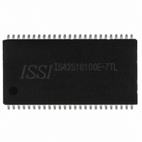
IS42S16100E-7TL ISSI, Integrated Silicon Solution Inc, IS42S16100E-7TL Datasheet - Page 21

IS42S16100E-7TL
Manufacturer Part Number
IS42S16100E-7TL
Description
IC SDRAM 16MBIT 143MHZ 50TSOP
Manufacturer
ISSI, Integrated Silicon Solution Inc
Type
SDRAMr
Specifications of IS42S16100E-7TL
Format - Memory
RAM
Memory Type
SDRAM
Memory Size
16M (1M x 16)
Speed
143MHz
Interface
Parallel
Voltage - Supply
3 V ~ 3.6 V
Operating Temperature
0°C ~ 70°C
Package / Case
50-TSOPII
Organization
1Mx16
Density
16Mb
Address Bus
12b
Access Time (max)
6/5.5ns
Maximum Clock Rate
143MHz
Operating Supply Voltage (typ)
3.3V
Package Type
TSOP-II
Operating Temp Range
0C to 70C
Operating Supply Voltage (max)
3.6V
Operating Supply Voltage (min)
3V
Supply Current
130mA
Pin Count
50
Mounting
Surface Mount
Operating Temperature Classification
Commercial
Lead Free Status / RoHS Status
Lead free / RoHS Compliant
Other names
706-1071
IS42S16100E-7TL
IS42S16100E-7TL
Available stocks
Company
Part Number
Manufacturer
Quantity
Price
Company:
Part Number:
IS42S16100E-7TL
Manufacturer:
ISSI
Quantity:
6 545
Company:
Part Number:
IS42S16100E-7TL
Manufacturer:
ISSI
Quantity:
851
Company:
Part Number:
IS42S16100E-7TLI
Manufacturer:
ISSI
Quantity:
11 200
Company:
Part Number:
IS42S16100E-7TLI
Manufacturer:
ISSI
Quantity:
104
Part Number:
IS42S16100E-7TLI
Manufacturer:
ISSI
Quantity:
20 000
IS42S16100E, IC42S16100E
Device Initialization At Power-On
(Power-On Sequence)
As is the case with conventional DRAMs, the IS42S16100E/
IC42S16100E product must be initialized by executing a
stipulated power-on sequence after power is applied.
After power is applied and Vdd and VddQ reach their
stipulated voltages, set and hold the CKE and DQM pins
HIGH for 100 µs. Then, execute the precharge command
to precharge both bank. Next, execute the auto-refresh
command twice or more and define the device operation
mode by executing a mode register set command.
The mode register set command can be also set before
auto-refresh command.
Mode Register Settings
The mode register set command sets the mode register.
When this command is executed, pins A0 to A9, A10, and
A11 function as data input pins for setting the register, and
this data becomes the device internal OP code. This OP
code has four fields as listed in the table below.
Note that the mode register set command can be executed
only when both banks are in the idle (inactive) state. Wait
at least two cycles after executing a mode register set
command before executing the next command.
CAS Latency
During a read operation, the between the execution of the
read command and data output is stipulated as the CAS
latency. This period can be set using the mode register
set command. The optimal CAS latency is determined
by the clock frequency and device speed grade. See the
“Operating Frequency / Latency Relationships” item for
details on the relationship between the clock frequency
and the CAS latency. See the table on the next page for
details on setting the mode register.
Integrated Silicon Solution, Inc. — www.issi.com
Rev. C
01/22/08
A11, A10, A9, A8, A7
A6, A5, A4
A2, A1, A0
Input Pin
A3
Mode Options
CAS Latency
Burst Length
Burst Type
Field
Burst Length
When writing or reading, data can be input or output data
continuously. In these operations, an address is input only
once and that address is taken as the starting address
internally by the device. The device then automatically
generates the following address. The burst length field in
the mode register stipulates the number of data items input
or output in sequence. In the IS42S16100E/IC42S16100E
product, a burst length of 1, 2, 4, 8, or full page can be
specified. See the table on the next page for details on
setting the mode register.
Burst Type
The burst data order during a read or write operation is
stipulated by the burst type, which can be set by the mode
register set command. The IS42S16100E/IC42S16100E
product supports sequential mode and interleaved mode
burst type settings. See the table on the next page for
details on setting the mode register. See the “Burst Length
and Column Address Sequence” item for details on DQ
data orders in these modes.
Write Mode
Burst write or single write mode is selected by the OP code
(A11, A10, A9) of the mode register.
A burst write operation is enabled by setting the OP code
(A11, A10, A9) to (0,0,0). A burst write starts on the same
cycle as a write command set. The write start address is
specified by the column address and bank select address
at the write command set cycle.
A single write operation is enabled by setting OP code (A11,
A10, A9) to (0, 0,1). In a single write operation, data is only
written to the column address and bank select address
specified by the write command set cycle without regard
to the bust length setting.
21


