NLSV1T34AMX1TCG ON Semiconductor, NLSV1T34AMX1TCG Datasheet
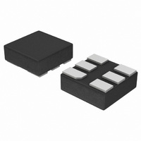
IC XLATOR 1BIT NON-INV 6ULLGA

NLSV1T34AMX1TCG

Manufacturer Part Number
NLSV1T34AMX1TCG
Description
IC XLATOR 1BIT NON-INV 6ULLGA
Manufacturer
ON Semiconductor
Datasheet

Specifications of NLSV1T34AMX1TCG

Logic Function
Translator
Number Of Bits
1
Input Type
Voltage
Output Type
Voltage
Number Of Channels
1
Number Of Outputs/channel
1
Differential - Input:output
No/No
Propagation Delay (max)
1.6ns
Voltage - Supply
0.9 V ~ 4.5 V
Operating Temperature
-40°C ~ 85°C
Package / Case
6-ULLGA
Supply Voltage
*
Low Level Output Current
24mA
Abs. Propagation Delay Time
3.3ns
Mounting
Surface Mount
Pin Count
6
Operating Temperature (min)
-40C
Operating Temperature (max)
85C
Operating Temperature Classification
Industrial
Logic Type
Dual Supply Translators
Supply Voltage (max)
4.5 V
Supply Voltage (min)
0.9 V
Maximum Operating Temperature
+ 85 C
Minimum Operating Temperature
- 40 C
Mounting Style
Screw
Number Of Circuits
2
High Level Output Current
-24mA
Operating Supply Voltage (typ)
1.8/2.5/3.3V
Operating Supply Voltage (max)
4.5V
Operating Supply Voltage (min)
0.9V
Lead Free Status / RoHS Status
Lead free / RoHS Compliant
Data Rate
-
Lead Free Status / Rohs Status
Compliant

Available stocks

Company
Part Number
Manufacturer
Quantity
Price
Part Number:
NLSV1T34AMX1TCG
Quantity:
795
Part Number:
NLSV1T34AMX1TCG
0
Company:
Part Number:
NLSV1T34AMX1TCG
Quantity:
2 500
Company:
Part Number:
NLSV1T34AMX1TCG
Quantity:
60 000
Company:
Part Number:
NLSV1T34AMX1TCG
Quantity:
1 138
NLSV1T34
1-Bit Dual-Supply
Non-Inverting Level
Translator
translator. The input A
different power supply rails, V
supply rails are configurable from 0.9 V to 4.5 V allowing universal
low−voltage translation from the input A
Features
Typical Applications
Important Information
© Semiconductor Components Industries, LLC, 2010
August, 2010 − Rev. 7
The NLSV1T34 is a 1−bit configurable dual−supply voltage level
Wide V
High−Speed w/ Balanced Propagation Delay
Inputs and Outputs have OVT Protection to 4.5 V
Non−preferential V
Power−Off Protection
Power−Off High Impedance Inputs and Outputs
Ultra−Small Packaging:
These are Pb−Free Devices
Mobile Phones, PDAs, Other Portable Devices
ESD Protection for All Pins:
A
CCA
HBM (Human Body Model) > 3000 V
V
and V
CCA
Figure 1. Logic Diagram
CCB
CCA
n
and output B
Operating Range: 0.9 V to 4.5 V
and V
1.45 mm x 1.0 mm ULLGA6
2.0 mm x 2.1 mm SC−88A
1.2 mm x 1.0 mm UDFN6
1.45 mm x 1.0 mm UDFN6
CCB
CCA
V
n
Sequencing
CCB
and V
ports are designed to track two
n
to the output B
CCB
respectively. Both
B
n
port.
1
See detailed ordering and shipping information in the package
dimensions section on page 5 of this data sheet.
V
GND
5
*Date Code orientation and/or position may vary
CCA
depending upon manufacturing location.
A
1
1
1
ULLGA6/UDFN6
1
(Note: Microdot may be in either location)
1
2
3
(Top View)
ORDERING INFORMATION
Q, A = Device Code
M
G
(SOT−353/SC−70)
http://onsemi.com
PIN ASSIGNMENT
CASE 517AQ
CASE 517AA
CASE 613AF
MX1 SUFFIX
6
5
4
CASE 419A
MU SUFFIX
MU SUFFIX
DF SUFFIX
ULLGA6
SC−88A
= Date Code*
= Pb−Free Package
UDFN6
UDFN6
V
NC
B
CCB
Publication Order Number:
V
GND
CCA
A
1
2
3
(Top View)
SC−88A
DIAGRAMS
MARKING
5
1
NLSV1T34/D
A M
QM
M
G
Q M G
5
4
G
V
B
CCB

Related parts for NLSV1T34AMX1TCG

NLSV1T34AMX1TCG Summary of contents

Page 1

NLSV1T34 1-Bit Dual-Supply Non-Inverting Level Translator The NLSV1T34 is a 1−bit configurable dual−supply voltage level translator. The input A and output different power supply rails, V CCA supply rails are configurable from 0 4.5 V ...

Page 2

PIN ASSIGNMENT PIN FUNCTION V Input Port DC Power Supply CCA V Output Port DC Power Supply CCB GND Ground A Input Port B Output Port MAXIMUM RATINGS Symbol Rating Supply Voltage CCA CCB V DC ...

Page 3

DC ELECTRICAL CHARACTERISTICS Symbol Parameter V Input HIGH Voltage IH V Input LOW Voltage IL V Output HIGH Voltage OH V Output LOW Voltage OL I Input Leakage Current I I Quiescent Supply Current CCA I Quiescent Supply Current CCB ...

Page 4

TOTAL STATIC POWER CONSUMPTION (I 4.5 V (V) Min Max CCA 4.5 2 3.3 2 2.8 < 2 1.8 < 1 0.9 < 0.5 NOTE: Connect ground before applying supply voltage and V will not damage the ...

Page 5

... Figure 3. AC (Propagation Delay) Test Circuit Waveforms Symbol ORDERING INFORMATION Device NLSV1T34MUTBG NLSV1T34AMUTCG NLSV1T34AMX1TCG NLSV1T34DFT2G †For information on tape and reel specifications, including part orientation and tape sizes, please refer to our Tape and Reel Packaging Specifications Brochure, BRD8011/ DUT Figure 2. AC (Propagation Delay) Test Circuit ) Vm ...

Page 6

... C H SOLDERING FOOTPRINT* 0.50 0.0197 0.40 0.0157 *For additional information on our Pb−Free strategy and soldering details, please download the ON Semiconductor Soldering and Mounting Techniques Reference Manual, SOLDERRM/D. PACKAGE DIMENSIONS SC−88A, SOT−353, SC−70 CASE 419A−02 ISSUE J NOTES: 1. DIMENSIONING AND TOLERANCING PER ANSI Y14 ...

Page 7

... SEATING PLANE 0.40 PITCH *For additional information on our Pb−Free strategy and soldering details, please download the ON Semiconductor Soldering and Mounting Techniques Reference Manual, SOLDERRM/D. http://onsemi.com 7 NOTES: 1. DIMENSIONING AND TOLERANCING PER ASME Y14.5M, 1994. 2. CONTROLLING DIMENSION: MILLIMETERS. 3. DIMENSION b APPLIES TO PLATED TERMINAL AND IS MEASURED BETWEEN 0 ...

Page 8

... OUTLINE 0.53 b *For additional information on our Pb−Free strategy and soldering 0. details, please download the ON Semiconductor Soldering and 0.05 C NOTE 3 Mounting Techniques Reference Manual, SOLDERRM/D. http://onsemi.com 8 NOTES: 1. DIMENSIONING AND TOLERANCING PER ASME Y14.5M, 1994. 2. CONTROLLING DIMENSION: MILLIMETERS. 3. DIMENSION b APPLIES TO PLATED TERMINAL AND IS MEASURED BETWEEN 0 ...

Page 9

... B *For additional information on our Pb−Free strategy and soldering NOTE 3 0.05 C details, please download the ON Semiconductor Soldering and Mounting Techniques Reference Manual, SOLDERRM/D. N. American Technical Support: 800−282−9855 Toll Free USA/Canada Europe, Middle East and Africa Technical Support: Phone: 421 33 790 2910 Japan Customer Focus Center Phone: 81− ...

Related keywords