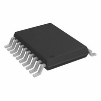
ADG3308BRUZ Analog Devices Inc, ADG3308BRUZ Datasheet - Page 15

ADG3308BRUZ
Manufacturer Part Number
ADG3308BRUZ
Description
IC XLATOR 8CH 1.2-5.5V 20-TSSOP
Manufacturer
Analog Devices Inc
Datasheet
1.ADG3308BCPZ-REEL7.pdf
(20 pages)
Specifications of ADG3308BRUZ
Logic Function
Translator, Bidirectional
Number Of Bits
8
Input Type
Logic
Output Type
Logic
Data Rate
50Mbps
Number Of Channels
1
Number Of Outputs/channel
1
Differential - Input:output
No/No
Propagation Delay (max)
6ns
Voltage - Supply
1.15 V ~ 5.5 V
Operating Temperature
-40°C ~ 85°C
Package / Case
20-TSSOP
Supply Voltage
1.15 V ~ 5.5 V
No. Of Inputs
8
Propagation Delay
6ns
Logic Type
Level Translator
Supply Voltage Range
1.15V To 5.5V
Logic Case Style
TSSOP
No. Of Pins
20
Operating Temperature Range
-40°C To +85°C
Lead Free Status / RoHS Status
Lead free / RoHS Compliant
Available stocks
Company
Part Number
Manufacturer
Quantity
Price
Part Number:
ADG3308BRUZ
Manufacturer:
ADI/亚德诺
Quantity:
20 000
TERMINOLOGY
V
Logic input high voltage at Pin A1 to Pin A8.
V
Logic input low voltage at Pin A1 to Pin A8.
V
Logic output high voltage at Pin A1 to Pin A8.
V
Logic output low voltage at Pin A1 to Pin A8.
C
Capacitance measured at Pin A1 to Pin A8 (EN = 0).
I
Leakage current at Pin A1 to Pin A8 when EN = 0 (high
impedance state at Pin A1 to Pin A8).
V
Logic input high voltage at Pin Y1 to Pin Y8.
V
Logic input low voltage at Pin Y1 to Pin Y8.
V
Logic output high voltage at Pin Y1 to Pin Y8.
V
Logic output low voltage at Pin Y1 to Pin Y8.
C
Capacitance measured at Pin Y1 to Pin Y8 (EN = 0).
I
Leakage current at Pin Y1 to Pin Y8 when EN = 0 (high
impedance state at Pin Y1 to Pin Y8).
V
Logic input high voltage at the EN pin.
V
Logic input low voltage at the EN pin.
C
Capacitance measured at EN pin.
I
Enable (EN) pin leakage current.
t
Three-state enable time for Pin A1 to Pin A8/Pin Y1 to Pin Y8.
t
Propagation delay when translating logic levels in the A→Y
direction.
t
Rise time when translating logic levels in the A→Y direction.
t
Fall time when translating logic levels in the A→Y direction.
EN
P, A→Y
R, A→Y
F, A→Y
LA, HIGH-Z
LY, HIGH-Z
LEN
A
Y
EN
IHA
ILA
OHA
OLA
IHY
ILY
OHY
OLY
IHEN
ILEN
Rev. C | Page 15 of 20
D
Guaranteed data rate when translating logic levels in the A→Y
direction under the driving and loading conditions specified in
Table 1.
t
Difference between propagation delays on any two channels
when translating logic levels in the A→Y direction.
t
Difference in propagation delay between any one channel and
the same channel on a different part (under same driving/
loading conditions) when translating in the A→Y direction.
t
Propagation delay when translating logic levels in the Y→A
direction.
t
Rise time when translating logic levels in the Y→A direction.
t
Fall time when translating logic levels in the Y→A direction.
D
Guaranteed data rate when translating logic levels in the Y→A
direction under the driving and loading conditions specified in
Table 1.
t
Difference between propagation delays on any two channels
when translating logic levels in the Y→A direction.
t
Difference in propagation delay between any one channel and
the same channel on a different part (under same driving/
loading conditions) when translating in the Y→A direction.
V
V
V
V
I
V
I
V
I
V
I
V
SKEW, A→Y
PPSKEW, A→Y
P, Y→A
R, Y→A
F, Y→A
SKEW, Y→A
PPSKEW, Y→A
CCA
CCY
HIGH-ZA
HIGH-ZY
CCA
CCA
CCY
CCY
CCA
CCY
CCA
CCY
MAX, A→Y
MAX, Y→A
supply voltage.
supply voltage.
supply current.
supply current.
supply current during three-state mode (EN = 0).
supply current during three-state mode (EN = 0).
ADG3308/ADG3308-1


