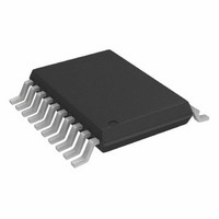
ADG3308BRUZ Analog Devices Inc, ADG3308BRUZ Datasheet

ADG3308BRUZ
Specifications of ADG3308BRUZ
Available stocks
Related parts for ADG3308BRUZ
ADG3308BRUZ Summary of contents
Page 1
FEATURES Bidirectional logic level translation Operates from 1. 5.5 V Low quiescent current < 1 μA No direction pin APPLICATIONS Low voltage ASIC level translation Smart card readers Cell phones and cell phone cradles Portable communication devices Telecommunications ...
Page 2
ADG3308/ADG3308-1 TABLE OF CONTENTS Features .............................................................................................. 1 Applications....................................................................................... 1 Functional Block Diagram .............................................................. 1 General Description ......................................................................... 1 Product Highlights ........................................................................... 1 Revision History ............................................................................... 2 Specifications..................................................................................... 3 Absolute Maximum Ratings............................................................ 6 ESD Caution.................................................................................. 6 Pin Configurations and Function Descriptions ...
Page 3
SPECIFICATIONS CCY CCA Table 1. Parameter LOGIC INPUTS/OUTPUTS A Side 3 Input High Voltage 3 Input Low Voltage Output High Voltage Output Low Voltage 3 Capacitance Leakage ...
Page 4
ADG3308/ADG3308-1 Parameter 1.8 V ± 0.15 V ≤ V ≤ 3.3 V ± 0.3 V CCA CCY CCY A→Y Level Translation Propagation Delay Rise Time Fall Time Maximum Data Rate Channel-to-Channel Skew Part-to-Part Skew Y→A Level ...
Page 5
Parameter 2.5 V ± 0.2 V ≤ V ≤ 3.3 V ± 0.3 V CCA CCY CCY A→Y Level Translation Propagation Delay Rise Time Fall Time Maximum Data Rate Channel-to-Channel Skew Part-to-Part Skew Y→A Level Translation ...
Page 6
ADG3308/ADG3308-1 ABSOLUTE MAXIMUM RATINGS T = 25°C, unless otherwise noted. A Table 2. Parameter V to GND CCA V to GND CCY Digital Inputs (A) Digital Inputs ( GND Operating Temperature Range Extended Industrial Range (B Version) Storage ...
Page 7
PIN CONFIGURATIONS AND FUNCTION DESCRIPTIONS CCA CCY ADG3308 TOP VIEW (Not to Scale ...
Page 8
ADG3308/ADG3308-1 TYPICAL PERFORMANCE CHARACTERISTICS 1 25° CHANNEL 0 50pF L 0 3.3V, V CCA CCY 0.7 0.6 0.5 0.4 V CCA 0.3 0.2 0 1.2V, V CCA ...
Page 9
T = 25° CHANNEL 1.8V CCA V = 3.3V CCY 7 50Mbps CAPACITIVE LOAD (pF) Figure 11. I vs. Capacitive Load ...
Page 10
ADG3308/ADG3308 25° CHANNEL 9 DATA RATE = 50kbps 1.2V 1.8V CCA CCY CCA CCA ...
Page 11
T = 25°C A DATA RATE = 25Mbps C = 50pF L 1 CHANNEL 400mV/DIV 5ns/DIV Figure 23. Eye Diagram at Y Output (1.2 V→1.8 V Level Translation, 25 Mbps 25° 50pF A L DATA RATE ...
Page 12
ADG3308/ADG3308-1 TEST CIRCUITS ADG3308/ V ADG3308-1 / CCA ADG3308-2 0.1µ GND Figure 29 Voltages at Pin ADG3308/ V CCA ADG3308-1 / ADG3308-2 0.1µ GND Figure 30. ...
Page 13
A→Y DIRECTION V CCA + 0.1µF 10µ SIGNAL SOURCE Z = 50Ω 50Ω 50Ω Y→A DIRECTION V CCA + 0.1µF 10µF 1MΩ 15pF 1MΩ SIGNAL ...
Page 14
ADG3308/ADG3308-1 SIGNAL SOURCE 50% 90% 50% 10% 0.1µF 50% 90% 50% 10% ADG3308/ V ADG3308-1 / CCA ADG3308-2 + 0.1µF 10µ 50Ω 50Ω T 50Ω GND ...
Page 15
TERMINOLOGY V IHA Logic input high voltage at Pin A1 to Pin A8. V ILA Logic input low voltage at Pin A1 to Pin A8. V OHA Logic output high voltage at Pin A1 to Pin A8. V OLA Logic ...
Page 16
ADG3308/ADG3308-1 THEORY OF OPERATION The ADG3308/ADG3308-1/ADG3308-2 level translators allow the level shifting necessary for data transfer in a system where multiple supply voltages are used. The device requires two supplies, V and V (V ≤ These supplies set ...
Page 17
DATA RATE The maximum data rate at which the device is guaranteed to operate is a function of the V and V CCA combination and the load capacitance. It represents the maximum frequency of a square wave that can be ...
Page 18
ADG3308/ADG3308-1 APPLICATIONS The ADG3308/ADG3308-1/ADG3308-2 are designed for digital circuits that operate at different supply voltages; therefore, logic level translation is required. The lower voltage logic signals are connected to the A pins, and the higher voltage logic signals to the ...
Page 19
OUTLINE DIMENSIONS COPLANARITY PIN 1 INDICATOR 12° MAX 1.00 0.85 0.80 SEATING PLANE 6.60 6.50 6. 4.50 4.40 4.30 6.40 BSC 1 10 PIN 1 0.65 BSC 1.20 MAX 0.15 0.20 0.05 0.09 0.30 0.19 SEATING 0.10 PLANE ...
Page 20
... Figure 45. Backside-Coated 20-Ball Wafer Level Chip Scale Package [WLCSP] ORDERING GUIDE Model Temperature Range 1 ADG3308BRUZ −40°C to +85°C 1 ADG3308BRUZ-REEL −40°C to +85°C 1 ADG3308BRUZ-REEL7 −40°C to +85°C ADG3308BCPZ-REEL 1 −40°C to +85°C 1 ADG3308BCPZ-REEL7 −40°C to +85°C 1 ADG3308BCBZ-1-RL7 −40°C to +85°C ...


