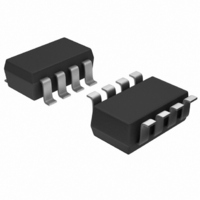
ADG3242BRJ-R2 Analog Devices Inc, ADG3242BRJ-R2 Datasheet

ADG3242BRJ-R2
Specifications of ADG3242BRJ-R2
Related parts for ADG3242BRJ-R2
ADG3242BRJ-R2 Summary of contents
Page 1
FEATURES 225 ps propagation delay through the switch 4.5 Ω switch connection between ports Data rate 1.5 Gbps 2.5 V/3.3 V supply operation Selectable level shifting/translation Level translation 3 2 1.8 V 2.5 V ...
Page 2
ADG3242 TABLE OF CONTENTS Features .............................................................................................. 1 Applications....................................................................................... 1 Functional Block Diagram .............................................................. 1 General Description ......................................................................... 1 Product Highlights ........................................................................... 1 Revision History ............................................................................... 2 Specifications..................................................................................... 3 Absolute Maximum Ratings............................................................ 4 ESD Caution.................................................................................. 4 Pin Configurations and Function Descriptions ...
Page 3
SPECIFICATIONS 3.6 V, GND = 0 V; all specifications T CC Table 1. Parameter DC ELECTRICAL CHARACTERISTICS Input High Voltage Input Low Voltage Input Leakage Current Off State Leakage Current On State Leakage Current Maximum ...
Page 4
ADG3242 ABSOLUTE MAXIMUM RATINGS T = 25°C, unless otherwise noted. A Table 2. Parameter V to GND CC Digital Inputs to GND DC Input Voltage DC Output Current Operating Temperature Range Industrial (B Version) Storage Temperature Range Junction Temperature θ ...
Page 5
PIN CONFIGURATIONS AND FUNCTION DESCRIPTIONS ADG3242 TOP VIEW (Not to Scale) GND 4 5 Figure 2. Pin Configuration Table 3. Pin Function Descriptions Pin No. Mnemonic ...
Page 6
ADG3242 TYPICAL PERFORMANCE CHARACTERISTICS 25°C A SEL = 0.5 1.0 1 Figure 4. On Resistance vs. Input Voltage 40 T ...
Page 7
T = 25° SEL = –5µA O 2.0 1 2.3V CC 1.0 0 0.5 1.0 1 Figure 10. Pass Voltage vs. V ...
Page 8
ADG3242 –1 –2 –3 – 25°C A – 3.3V/2.5V CC SEL = V CC – 0dBm IN N/W ANALYZER: – 50Ω –8 0.03 0.1 1 ...
Page 9
V = SEL = 3. 1.5V p-p IN 20dB ATTENUATION EYE WIDTH = ((CLOCK PERIOD – JITTER p-p)/CLOCK PERIOD) × 100% 50 0.5 0.7 0.9 1.1 ...
Page 10
ADG3242 TERMINOLOGY V CC Positive power supply voltage. GND Ground (0 V) reference. V INH Minimum input voltage for Logic 1. V INL Maximum input voltage for Logic Input leakage current at the control inputs ...
Page 11
TIMING MEASUREMENT INFORMATION For the following load circuit and waveforms, the notation that is used is V and V where: IN OUT and OUT ...
Page 12
ADG3242 BUS SWITCH APPLICATIONS MIXED VOLTAGE OPERATION, LEVEL TRANSLATION Bus switches provide an ideal solution for interfacing between mixed voltage systems. The ADG3242 is suitable for applications where voltage translation from 3.3 V technology to a lower voltage technology is ...
Page 13
BUS ISOLATION A common requirement of bus architectures is low capacitance loading of the bus. Such systems require bus bridge devices that extend the number of loads on the bus without exceeding the spec- ifications. Because the ADG3242 is designed ...
Page 14
... ADG3242 OUTLINE DIMENSIONS INDICATOR 0.15 MAX ORDERING GUIDE Model Temperature Range ADG3242BRJ-R2 −40°C to +85°C ADG3242BRJ-REEL −40°C to +85°C ADG3242BRJ-REEL7 −40°C to +85°C 1 ADG3242BRJZ-REEL7 −40°C to +85°C 1 ADG3242BCZ-SF3 −40°C to +85° Pb-free part. 2.90 BSC 1.60 BSC 2 ...
Page 15
NOTES Rev Page ADG3242 ...
Page 16
ADG3242 NOTES ©2006 Analog Devices, Inc. All rights reserved. Trademarks and registered trademarks are the property of their respective owners. C04309-0-9/06(A) Rev Page ...


