74F673APC Fairchild Semiconductor, 74F673APC Datasheet

IC REGISTER SHIFT 16BIT 24-DIP

74F673APC

Manufacturer Part Number
74F673APC
Description
IC REGISTER SHIFT 16BIT 24-DIP
Manufacturer
Fairchild Semiconductor
Series
74Fr
Datasheet

Specifications of 74F673APC

Logic Type
Shift Register
Output Type
Standard
Number Of Elements
1
Number Of Bits Per Element
16
Function
Serial to Parallel
Voltage - Supply
4.5 V ~ 5.5 V
Operating Temperature
0°C ~ 70°C
Mounting Type
Through Hole
Package / Case
24-DIP (0.600", 15.24mm)
Lead Free Status / RoHS Status
Lead free / RoHS Compliant
Other names
74F673
© 2000 Fairchild Semiconductor Corporation
74F673ASC
74F673APC
74F673ASPC
74F673A
16-Bit Serial-In, Serial/Parallel-Out Shift Register
General Description
The 74F673A contains a 16-bit serial-in, serial-out shift
register and a 16-bit Parallel-Out storage register. A single
pin serves either as an input for serial entry or as a
3-STATE serial output. In the Serial-Out mode, the data
recirculates in the shift register. By means of a separate
clock, the contents of the shift register are transferred to
the storage register for parallel outputting. The contents of
the storage register can also be parallel loaded back into
the shift register. A HIGH signal on the Chip Select input
prevents both shifting and parallel transfer. The storage
register may be cleared via STMR.
Ordering Code:
Devices also available in Tape and Reel. Specify by appending the suffix letter “X” to the ordering code.
Logic Symbols
Order Number
Package Number
IEEE/IEC
M24B
N24C
N24A
24-Lead Small Outline Integrated Circuit (SOIC), JEDEC MS-013, 0.300 Wide
24-Lead Plastic Dual-In-Line Package (PDIP), JEDEC MS-011, 0.600 Wide
24-Lead Plastic Dual-In-Line Package (PDIP), JEDEC MS-001, 0.300 Wide
DS009585
Features
Connection Diagram
Serial-to-parallel converter
16-bit serial I/O shift register
16-bit parallel-out storage register
Recirculating serial shifting
Recirculating parallel transfer
Common serial data I/O pin
Slim 24 lead package
Package Description
April 1988
Revised October 2000
www.fairchildsemi.com

Related parts for 74F673APC

74F673APC Summary of contents

Page 1

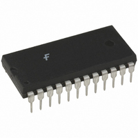
... Ordering Code: Order Number Package Number 74F673ASC M24B 24-Lead Small Outline Integrated Circuit (SOIC), JEDEC MS-013, 0.300 Wide 74F673APC N24A 24-Lead Plastic Dual-In-Line Package (PDIP), JEDEC MS-011, 0.600 Wide 74F673ASPC N24C 24-Lead Plastic Dual-In-Line Package (PDIP), JEDEC MS-001, 0.300 Wide Devices also available in Tape and Reel. Specify by appending the suffix letter “X” to the ordering code. ...

Page 2

Unit Loading/Fan Out Pin Names CS Chip Select Input (Active LOW) SHCP Shift Clock Pulse Input (Active Falling Edge) STMR Store Master Reset Input (Active LOW) STCP Store Clock Pulse Input R/W Read/Write Input SI/O Serial Data Input or 3-STATE ...

Page 3

Block Diagram 3 www.fairchildsemi.com ...

Page 4

Absolute Maximum Ratings Storage Temperature Ambient Temperature under Bias Junction Temperature under Bias V Pin Potential to Ground Pin CC Input Voltage (Note 2) Input Current (Note 5.0 mA Voltage Applied to Output in HIGH State ...

Page 5

AC Electrical Characteristics Symbol Parameter f Maximum Clock Frequency MAX t Propagation Delay PLH t STCP to Q PHL n t Propagation Delay PHL STMR Propagation Delay PLH t SHCP to SI/O PHL t Output Enable ...

Page 6

Physical Dimensions inches (millimeters) unless otherwise noted 24-Lead Small Outline Integrated Circuit (SOIC), JEDEC MS-013, 0.300 Wide 24-Lead Plastic Dual-In-Line Package (PDIP), JEDEC MS-011, 0.600 Wide www.fairchildsemi.com Package Number M24B Package Number N24A 6 ...

Page 7

Physical Dimensions inches (millimeters) unless otherwise noted (Continued) 24-Lead Plastic Dual-In-Line Package (PDIP), JEDEC MS-001, 0.300 Wide Fairchild does not assume any responsibility for use of any circuitry described, no circuit patent licenses are implied and Fairchild reserves the right ...

Related keywords