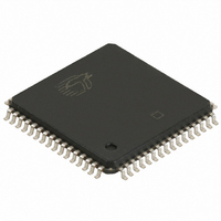
CY7C4245-10ASXC Cypress Semiconductor Corp, CY7C4245-10ASXC Datasheet - Page 6

CY7C4245-10ASXC
Manufacturer Part Number
CY7C4245-10ASXC
Description
IC SYNC FIFO MEM 4KX18 64LQFP
Manufacturer
Cypress Semiconductor Corp
Series
CY7Cr
Datasheet
1.CY7C4245-15JXC.pdf
(22 pages)
Specifications of CY7C4245-10ASXC
Function
Synchronous
Memory Size
72K (4K x 18)
Data Rate
100MHz
Access Time
8ns
Voltage - Supply
3.3V
Operating Temperature
-40°C ~ 85°C
Mounting Type
Surface Mount
Package / Case
64-LQFP
Lead Free Status / RoHS Status
Lead free / RoHS Compliant
Available stocks
Company
Part Number
Manufacturer
Quantity
Price
Company:
Part Number:
CY7C4245-10ASXC
Manufacturer:
Cypress Semiconductor Corp
Quantity:
10 000
Company:
Part Number:
CY7C4245-10ASXCT
Manufacturer:
Cypress Semiconductor Corp
Quantity:
10 000
Width Expansion Configuration
The CY7C42X5 can be expanded in width to provide word widths
greater than 18 in increments of 18. During width expansion
mode all control line inputs are common and all flags are
Depth Expansion Configuration (with Program-
mable Flags)
The CY7C42X5 can easily be adapted to applications requiring
more than 64/256/512/1024/2048/4096 words of buffering.
Figure 4
Maximum depth is limited only by signal loading. Follow these
steps:
Document Number: 001-45652 Rev. **
1. The first device must be designated by grounding the First
2. All other devices must have FL in the HIGH state.
3. The Write Expansion Out (WXO) pin of each device must be
4. The Read Expansion Out (RXO) pin of each device must be
5. All Load (LD) pins are tied together.
6. The Half-Full Flag (HF) is not available in the Depth
7. EF, FF, PAE, and PAF are created with composite flags by
Load (FL) control input.
tied to the Write Expansion In (WXI) pin of the next device.
tied to the Read Expansion In (RXI) pin of the next device.
Expansion Configuration.
ORing together these respective flags for monitoring. The
composite PAE and PAF flags are not precise.
FULL FLAG (FF)
PROGRAMMABLE(PAE)
DATAIN (D)
WRITE CLOCK (WCLK)
WRITE ENABLE (WEN)
HALF FULL FLAG (HF)
shows Depth Expansion using three CY7C42X5s.
Figure 3. Block Diagram of Synchronous FIFO Memories Used in a Width Expansion Configuration
LOAD (LD)
36
18
WRITE EXPANSION IN (WXI)
READ EXPANSION IN (RXI)
FIRST LOAD (FL)
FF
RESET (RS)
7C4425
7C4205
7C4215
7C4225
7C4235
7C4245
EF
18
18
available. Empty (Full) flags should be created by ANDing the
Empty (Full) flags of every FIFO. This technique will avoid ready
data from the FIFO that is “staggered” by one clock cycle due to
the variations in skew between RCLK and WCLK.
demonstrates a 36-word width by using two CY7C42X5.
WRITE EXPANSION IN (WXI)
READ EXPANSION IN (RXI)
FF
FIRST LOAD (FL)
RESET (RS)
7C4425
7C4205
7C4215
7C4225
7C4235
7C4245
EF
CY7C4425/4205/4215
CY7C4225/4235/4245
18
READ CLOCK (RCLK)
READ ENABLE (REN)
OUTPUT ENABLE(OE)
PROGRAMMABLE(PAF)
DATAOUT (Q)
EMPTYFLAG (EF)
Page 6 of 22
36
Figure 3
[+] Feedback


